SCLS985 January 2024 SN74LV4T125-EP
PRODUCTION DATA
- 1
- 1 Features
- 2 Applications
- 3 Description
- 4 Additional Product Selection
- 5 Pin Configuration and Functions
- 6 Specifications
- 7 Parameter Measurement Information
- 8 Detailed Description
- 9 Applications and Implementation
- 10Device and Documentation Support
- 11Revision History
- 12Mechanical, Packaging, and Orderable Information
Package Options
Mechanical Data (Package|Pins)
- PW|14
Thermal pad, mechanical data (Package|Pins)
Orderable Information
3 Description
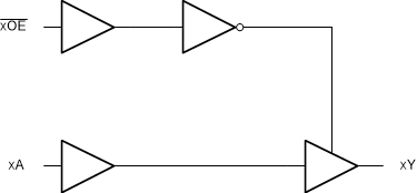
The SN74LV4T125-EP contains four independent buffers with 3-state outputs and extended voltage operation to allow for level translation. Each buffer performs the Boolean function Y = A in positive logic. The outputs can be put into a high impedance (Hi-Z) state by applying a HIGH on the OE pin. The output level is referenced to the supply voltage (VCC) and supports 1.8V, 2.5V, 3.3V, and 5V CMOS levels.
The input is designed with a lower threshold circuit to support up translation for lower voltage CMOS inputs (for example, 1.2V input to 1.8V output or 1.8V input to 3.3V output). In addition, the 5V tolerant input pins enable down translation (for example, 3.3V to 2.5V output).
| PART NUMBER(1) | PACKAGE(2) | PACKAGE SIZE(3) | BODY SIZE (NOM)(4) |
|---|---|---|---|
| SN74LV4T125-EP | PW (TSSOP, 14) | 5 mm × 6.4 mm | 5 mm × 4.4 mm |
 Simplified Logic Diagram
(Positive Logic)