SCLS749C February 2014 – June 2022 SN74LV4T125
PRODUCTION DATA
- 1 Features
- 2 Applications
- 3 Description
- 4 Revision History
- 5 Pin Configuration and Functions
- 6 Specifications
- 7 Parameter Measurement Information
- 8 Detailed Description
- 9 Applications and Implementation
- 10Power Supply Recommendations
- 11Layout
- 12Device and Documentation Support
- 13Mechanical, Packaging, and Orderable Information
Package Options
Mechanical Data (Package|Pins)
Thermal pad, mechanical data (Package|Pins)
Orderable Information
3 Description
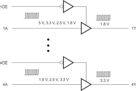
SN74LV4T125 is a low-voltage CMOS buffer gate that operates at a wider voltage range for portable, telecom, industrial, and automotive applications. The output level is referenced to the supply voltage and is able to support 1.8-V, 2.5-V, 3.3-V, and 5-V CMOS levels.
The input is designed with a lower threshold circuit to match 1.8-V input logic at VCC = 3.3 V and can be used in 1.8 V to 3.3 V level-up translation. In addition, the 5-V tolerant input pins enable down translation (for example, 3.3 V to 2.5 V output at VCC = 2.5 V). The wide VCC range of 1.8 V to 5.5 V allows the generation of desired output levels to connect to controllers or processors.
The SN74LV4T125 device is designed with current-drive capability of 8 mA to reduce line reflections, overshoot, and undershoot caused by high-drive outputs.
| PART NUMBER (1) | PACKAGE | BODY SIZE (NOM) |
|---|---|---|
| SN74LV4T125 | PW (TSSOP, 14) | 5.00 mm x 4.40 mm |
| RGY (VQFN, 14) | 3.50 mm x 3.50 mm |
 Figure 3-1 Simplified Application Diagram