SCLS414T April 1998 – March 2023 SN74LV595A
PRODMIX
- 1 Features
- 2 Applications
- 3 Description
- 4 Revision History
- 5 Pin Configuration and Functions
-
6 Specifications
- 6.1 Absolute Maximum Ratings
- 6.2 ESD Ratings
- 6.3 Recommended Operating Conditions
- 6.4 Thermal Information
- 6.5 Electrical Characteristics
- 6.6 Timing Requirements, VCC = 2.5 V ± 0.2 V
- 6.7 Timing Requirements, VCC = 3.3 V ± 0.3 V
- 6.8 Timing Requirements, VCC = 5 V ± 0.5 V
- 6.9 Switching Characteristics, VCC = 2.5 V ± 0.2 V
- 6.10 Switching Characteristics, VCC = 3.3 V ± 0.3 V
- 6.11 Switching Characteristics, VCC = 5 V ± 0.5 V
- 6.12 Noise Characteristics
- 6.13 Operating Characteristics
- 6.14 Typical Characteristics
- 7 Parameter Measurement Information
- 8 Detailed Description
- 9 Application and Implementation
- 10Device and Documentation Support
- 11Mechanical, Packaging, and Orderable Information
Package Options
Mechanical Data (Package|Pins)
Thermal pad, mechanical data (Package|Pins)
- BQB|16
Orderable Information
5 Pin Configuration and Functions
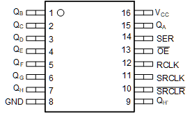
 Figure 5-1 D, DW, or PW Package,
16-Pin SOIC, SOP or TSSOP
(Top View)
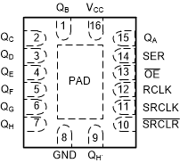
 Figure 5-2 BQB or RGY Package,
16-Pin WQFN or VQFN
(Transparent Top View)
Table 5-1 Pin Functions
| PIN | TYPE(1) | DESCRIPTION | ||
|---|---|---|---|---|
| NAME | NO. | |||
| GND | 8 | G | Ground Pin | |
| OE | 13 | I |
Output Enable Pin. Active LOW |
|
| QA | 15 | O | QA Output | |
| QB | 1 | O | QB Output | |
| QC | 2 | O | QC Output | |
| QD | 3 | O | QD Output | |
| QE | 4 | O | QE Output | |
| QF | 5 | O | QF Output | |
| QG | 6 | O | QG Output | |
| QH | 7 | O | QH Output | |
| QH' | 9 | O | QH' Output | |
| RCLK | 12 | I | RCLK Input | |
| SER | 14 | I | SER Input | |
| SRCLK | 11 | I | SRCLK Input | |
| SRCLR | 10 | I | SRCLR Input | |
| VCC | 16 | P | Power Pin | |
| Thermal Pad | — | Thermal Pad(2) | ||
(1) I = Input, O = Output, I/O =
Input or Output, G = Ground, P = Power
(2) RGY and BQB package only