SCLS556C december 2003 – august 2023 SN74LV74A-Q1
PRODUCTION DATA
- 1
- 1Features
- 2Description
- 3Revision History
- 4Pin Configuration and Functions
-
5Specifications
- 5.1 Absolute Maximum Ratings
- 5.2 ESD Ratings
- 5.3 Recommended Operating Conditions
- 5.4 Thermal Information
- 5.5 Electrical Characteristics
- 5.6 Timing Requirements, VCC = 2.5 V ±0.2 V
- 5.7 Timing Requirements, VCC = 3.3 V ±0.3 V
- 5.8 Timing Requirements, VCC = 5 V ±0.5 V
- 5.9 Switching Characteristics, VCC = 2.5 V ±0.2 V
- 5.10 Switching Characteristics, VCC = 3.3 V ±0.3 V
- 5.11 Switching Characteristics, VCC = 5 V ±0.5 V
- 5.12 Noise Characteristics
- 5.13 Operating Characteristics
- 6Parameter Measurement Information
- 7Detailed Description
- 8Device and Documentation Support
- 9Mechanical, Packaging, and Orderable Information
Package Options
Refer to the PDF data sheet for device specific package drawings
Mechanical Data (Package|Pins)
- D|14
- PW|14
Thermal pad, mechanical data (Package|Pins)
Orderable Information
4 Pin Configuration and Functions
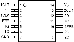
 Figure 4-1 D and PW Package
14-Pin SOIC and TSSOP
(Top View)
Table 4-1 Pin Functions
| PIN | TYPE1 | DESCRIPTION | |
|---|---|---|---|
| NO. | NAME | ||
| 1 | 1 CLR | I | 1 clear |
| 2 | 1D | I | 1D input |
| 3 | 1CLK | I | 1 clock |
| 4 | 1 PRE | I | 1 preset |
| 5 | 1Q | O | 1Q output |
| 6 | 1 Q | O | 1 Q output |
| 7 | GND | – | GND |
| 8 | 2 Q | O | 2 Q output |
| 9 | 2Q | O | 2Q output |
| 10 | 2 PRE | I | 2 preset |
| 11 | 2CLK | I | 2 clock |
| 12 | 2D | I | 2D input |
| 13 | 2 CLR | I | 2 clear |
| 14 | Vcc | – | Supply voltage input |
- Signal Types: I = Input, O = Output, I/O = Input or Output.