SCLS951A August   2023  – November 2023 SN74LV8T165-Q1

PRODUCTION DATA  

  1.   1
  2. Features
  3. Applications
  4. Description
  5. Pin Configuration and Functions
  6. Specifications
    1. 5.1 Absolute Maximum Ratings
    2. 5.2 ESD Ratings
    3. 5.3 Recommended Operating Conditions
    4. 5.4 Thermal Information
    5. 5.5 Electrical Characteristics
    6. 5.6 Timing Characteristics
    7. 5.7 Switching Characteristics
    8. 5.8 Typical Characteristics
  7. Parameter Measurement Information
  8. Detailed Description
    1. 7.1 Overview
    2. 7.2 Functional Block Diagram
    3. 7.3 Feature Description
      1. 7.3.1 LVxT Enhanced Input Voltage
        1. 7.3.1.1 Down Translation
        2. 7.3.1.2 Up Translation
      2. 7.3.2 Balanced CMOS Push-Pull Outputs
      3. 7.3.3 Latching Logic with Known Power-Up State
      4. 7.3.4 Clamp Diode Structure
    4. 7.4 Device Functional Modes
  9. Application and Implementation
    1. 8.1 Application Information
    2. 8.2 Typical Application
      1. 8.2.1 Design Requirements
        1. 8.2.1.1 Power Considerations
        2. 8.2.1.2 Input Considerations
        3. 8.2.1.3 Output Considerations
      2. 8.2.2 Detailed Design Procedure
      3. 8.2.3 Application Curves
    3. 8.3 Power Supply Recommendations
    4. 8.4 Layout
      1. 8.4.1 Layout Guidelines
      2. 8.4.2 Layout Example
  10. Device and Documentation Support
    1. 9.1 Documentation Support
      1. 9.1.1 Related Documentation
    2. 9.2 Receiving Notification of Documentation Updates
    3. 9.3 Support Resources
    4. 9.4 Trademarks
    5. 9.5 Electrostatic Discharge Caution
    6. 9.6 Glossary
  11. 10Revision History
  12. 11Mechanical, Packaging, and Orderable Information

Package Options

Refer to the PDF data sheet for device specific package drawings

Mechanical Data (Package|Pins)
  • BQB|16
  • PW|16
Thermal pad, mechanical data (Package|Pins)
Orderable Information

Description

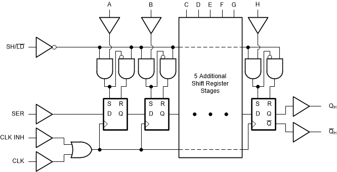
The SN74LV8T165-Q1 device is a parallel- or serial-in, serial-out 8-bit shift register. This device has two modes of operation: load data, and shift data which are controlled by the SH/LD input. The output level is referenced to the supply voltage (VCC) and supports 1.8-V, 2.5-V, 3.3-V, and 5-V CMOS levels.

The input is designed with a lower threshold circuit to support up translation for lower voltage CMOS inputs (for example 1.2 V input to 1.8 V output or 1.8 V input to 3.3 V output). In addition, the 5-V tolerant input pins enable down translation (for example 3.3 V to 2.5 V output).

Package Information
PART NUMBER PACKAGE(1) PACKAGE SIZE(2) BODY SIZE (NOM)(3)
SN74LV8T165-Q1 PW (TSSOP, 16) 5 mm × 6.4 mm 5 mm × 4.4 mm
BQB (WQFN, 16) 3.5 mm × 2.5 mm 3.5 mm × 2.5 mm
For more information, see Section 11
The package size (length × width) is a nominal value and includes pins, where applicable.
The body size (length × width) is a nominal value and does not include pins.
GUID-20210218-CA0I-X1MX-NFLV-2M5MCVCRVZZD-low.gifSimplified Logic Diagram (Positive Logic)