SCAS989 March 2024 SN74LV8T541-Q1
ADVANCE INFORMATION
- 1
- 1 Features
- 2 Applications
- 3 Description
- 4 Pin Configuration and Functions
- 5 Specifications
- 6 Parameter Measurement Information
- 7 Detailed Description
- 8 Feature Description
- 9 Device Functional Modes
- 10Application and Implementation
- 11Device and Documentation Support
- 12Revision History
- 13Mechanical, Packaging, and Orderable Information
Package Options
Refer to the PDF data sheet for device specific package drawings
Mechanical Data (Package|Pins)
- PW|20
Thermal pad, mechanical data (Package|Pins)
Orderable Information
3 Description
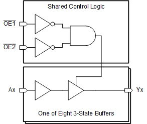
The SN74LV8T541-Q1
contains eight buffers with 3-state outputs. The active low output enable pins
(OE1 and OE2) control all eight channels,
and are configured so that both must be low for the outputs to be active.
 Simplified Logic Diagram (Positive Logic)
The input is designed with a reduced threshold circuit to support up translation when the supply voltage is larger than the input voltage. Additionally, the 5V tolerant input pins enable down translation when the input voltage is larger than the supply voltage. The output level is always referenced to the supply voltage (VCC) and supports 1.8V, 2.5V, 3.3V, and 5V CMOS levels.
Package Information
| PART NUMBER | PACKAGE(1) | PACKAGE SIZE(2) | BODY SIZE (NOM)(3) |
|---|---|---|---|
| SN74LV8T541-Q1 | PW (TSSOP, 20) | 6.5mm × 6.4mm | 6.5mm × 4.4mm |
(1) For more information, see Section 13.
(2) The package size (length × width) is a nominal value and includes
pins, where applicable.
(3) The body size (length × width) is a nominal value and does not
include pins.
 Simplified Logic Diagram (Positive Logic)