SCAS994 March 2024 SN74LV8T595
PRODUCTION DATA
- 1
- 1 Features
- 2 Applications
- 3 Description
- 4 Pin Configuration and Functions
- 5 Specifications
- 6 Parameter Measurement Information
- 7 Detailed Description
- 8 Application and Implementation
- 9 Device and Documentation Support
- 10Revision History
- 11Mechanical, Packaging, and Orderable Information
Package Options
Refer to the PDF data sheet for device specific package drawings
Mechanical Data (Package|Pins)
- BQB|16
- PW|16
Thermal pad, mechanical data (Package|Pins)
- BQB|16
Orderable Information
4 Pin Configuration and Functions
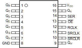
 Figure 4-1 PW Package, 16-Pin TSSOP (Top View)
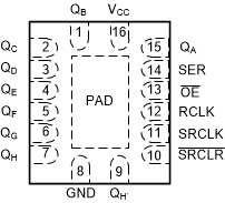
 Figure 4-2 BQB Package, 16-Pin WQFN
(Transparent Top View)
Figure 4-2 BQB Package, 16-Pin WQFN
(Transparent Top View)Table 4-1 Pin Functions
| PIN | TYPE(1) | DESCRIPTION | |
|---|---|---|---|
| NAME | NO. | ||
| QB | 1 | O | QB output |
| QC | 2 | O | QC output |
| QD | 3 | O | QD output |
| QE | 4 | O | QE output |
| QF | 5 | O | QF output |
| QG | 6 | O | QG output |
| QH | 7 | O | QH output |
| GND | 8 | G | Ground |
| QH' | 9 | O | Serial output, can be used for cascading |
| SRCLR | 10 | I | Shift register clear, active low |
| SRCLK | 11 | I | Shift register clock, rising edge triggered |
| RCLK | 12 | I | Output register clock, rising edge triggered |
| OE | 13 | I | Output Enable, active low |
| SER | 14 | I | Serial input |
| QA | 15 | O | QA output |
| VCC | 16 | P | Positive supply |
| Thermal Pad(2) | — | The thermal pad can be connect to GND or left floating. Do not connect to any other signal or supply. | |
(1) I = Input, O = Output, I/O = Input or Output, G = Ground, P = Power
(2) BQB package only