SCAS291W MARCH   1993  – October 2016 SN54LVC138A , SN74LVC138A

PRODUCTION DATA.  

  1. Features
  2. Applications
  3. Description
  4. Revision History
  5. Pin Configuration and Functions
  6. Specifications
    1. 6.1 Absolute Maximum Ratings
    2. 6.2 ESD Ratings
    3. 6.3 Recommended Operating Conditions
    4. 6.4 Thermal Information
    5. 6.5 Electrical Characteristics
    6. 6.6 Switching Characteristics—SN54LVC138A
    7. 6.7 Switching Characteristics—SN74LVC138A
    8. 6.8 Operating Characteristics
    9. 6.9 Typical Characteristics
  7. Parameter Measurement Information
  8. Detailed Description
    1. 8.1 Overview
    2. 8.2 Functional Block Diagram
    3. 8.3 Feature Description
      1. 8.3.1 3-Line to 8-Line Decoder
      2. 8.3.2 1.65-V to 3.6-V Operation With Inputs up to 5.5 V
    4. 8.4 Device Functional Modes
  9. Application and Implementation
    1. 9.1 Application Information
    2. 9.2 Typical Application
      1. 9.2.1 Design Requirements
      2. 9.2.2 Detailed Design Procedure
      3. 9.2.3 Application Curve
  10. 10Power Supply Recommendations
  11. 11Layout
    1. 11.1 Layout Guidelines
    2. 11.2 Layout Example
  12. 12Device and Documentation Support
    1. 12.1 Related Links
    2. 12.2 Receiving Notification of Documentation Updates
    3. 12.3 Community Resources
    4. 12.4 Trademarks
    5. 12.5 Electrostatic Discharge Caution
    6. 12.6 Glossary
  13. 13Mechanical, Packaging, and Orderable Information

Package Options

Refer to the PDF data sheet for device specific package drawings

Mechanical Data (Package|Pins)
  • DB|16
  • PW|16
  • NS|16
  • RGY|16
  • D|16
  • DGV|16
  • RSV|16
Thermal pad, mechanical data (Package|Pins)
Orderable Information

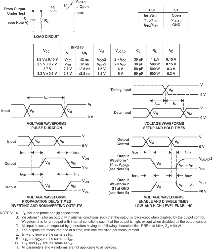
Parameter Measurement Information

SN54LVC138A SN74LVC138A pmi_cas291.gif Figure 2. Load Circuit and Voltage Waveforms