SCLSA17 May 2024 SN74LVC165A-Q1
PRODUCTION DATA
- 1
- 1 Features
- 2 Applications
- 3 Description
- 4 Pin Configuration and Functions
- 5 Specifications
- 6 Parameter Measurement Information
- 7 Detailed Description
- 8 Application and Implementation
- 9 Device and Documentation Support
- 10Revision History
- 11Mechanical, Packaging, and Orderable Information
Package Options
Refer to the PDF data sheet for device specific package drawings
Mechanical Data (Package|Pins)
- PW|16
- BQB|16
Thermal pad, mechanical data (Package|Pins)
- BQB|16
Orderable Information
3 Description
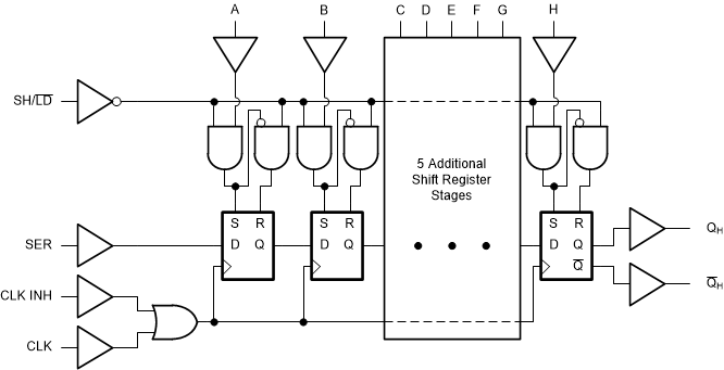
The SN74LVC165A-Q1 contains one 8-bit parallel-load shift register. Data is loaded asynchronously using the shift or load (SH/LD) select pin. The device includes a serial (SER) input to allow for daisy chaining, and a standard (QH) and inverted (QH) output.
Package
Information
| PART NUMBER | PACKAGE(1) | PACKAGE SIZE(2) | BODY SIZE (NOM)(3) |
|---|---|---|---|
| SN74LVC165A-Q1 | BQB (WQFN, 16) | 3.5mm × 2.5mm | 3.5mm × 2.5mm |
| D (SOIC, 16) | 9.9mm × 6mm | 9.9mm × 3.9mm | |
| PW (TSSOP, 16) | 5mm × 6.4mm | 5mm × 4.4mm |
(1) For more information, see Section 11.
(2) The package size (length × width) is a nominal value and includes
pins, where applicable
(3) The body size (length × width) is a nominal value and does not
include pins.
 Functional Diagram