SCES487I September 2003 – November 2024 SN74LVC1G11
PRODUCTION DATA
- 1
- 1 Features
- 2 Applications
- 3 Description
- 4 Pin Configuration and Functions
-
5 Specifications
- 5.1 Absolute Maximum Ratings
- 5.2 ESD Ratings
- 5.3 Recommended Operating Conditions
- 5.4 Thermal Information
- 5.5 Electrical Characteristics
- 5.6 Switching Characteristics, CL = 15 pF
- 5.7 Switching Characteristics, CL = 30 pF or 50 pF
- 5.8 Switching Characteristics, CL = 30 pF or 50 pF
- 5.9 Operating Characteristics
- 5.10 Typical Characteristics
- 6 Parameter Measurement Information
- 7 Detailed Description
- 8 Application and Implementation
- 9 Device and Documentation Support
- 10Revision History
- 11Mechanical, Packaging, and Orderable Information
Package Options
Refer to the PDF data sheet for device specific package drawings
Mechanical Data (Package|Pins)
- DBV|6
- DSF|6
- YZP|6
- DCK|6
- DRY|6
Thermal pad, mechanical data (Package|Pins)
- DRY|6
Orderable Information
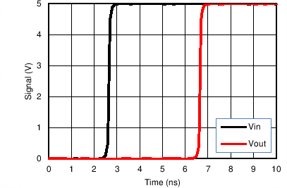
8.2.3 Application Curve

| VCC = 5 V | ||