SCES586E July 2004 – March 2024 SN74LVC1G123
PRODUCTION DATA
- 1
- 1 Features
- 2 Applications
- 3 Description
- 4 Pin Configuration and Functions
-
5 Specifications
- 5.1 Absolute Maximum Ratings
- 5.2 ESD Ratings
- 5.3 Recommended Operating Conditions
- 5.4 Thermal Information
- 5.5 Electrical Characteristics
- 5.6 Timing Requirements
- 5.7 Switching Characteristics, CL = 15 pF, –40°C to 85°C
- 5.8 Switching Characteristics, CL = 50 pF, –40°C to 85°C
- 5.9 Switching Characteristics, CL = 50 pF, –40°C to 125°C
- 5.10 Operating Characteristics
- 5.11 Typical Characteristics
- 6 Parameter Measurement Information
- 7 Detailed Description
- 8 Application and Implementation
- 9 Power Supply Recommendations
- 10Layout
- 11Device and Documentation Support
- 12Revision History
- 13Mechanical, Packaging, and Orderable Information
Package Options
Mechanical Data (Package|Pins)
Thermal pad, mechanical data (Package|Pins)
Orderable Information
4 Pin Configuration and Functions

See mechanical
drawings for dimensions.
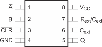
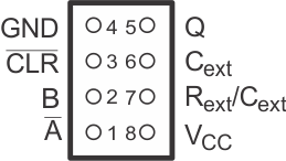
Figure 4-1 DCT Package8-Pin SSOPTop View Figure 4-2 DCU Package8-Pin VSSOPTop View
 Figure 4-3 YZP Package8-Pin DSBGABottom View
Table 4-1 Pin Functions
| PIN | I/O | DESCRIPTION | |
|---|---|---|---|
| NAME | NO. | ||
| A | 1 | I | Falling edge sensitive input; requires B and CLR to be held high. |
| B | 2 | I | Rising edge sensitive input; requires A to be held low and CLR to be held high. |
| CLR | 3 | I | Clear, Active Low; also can operate as rising edge sensitive input if A is held low and B is held high. |
| GND | 4 | — | Ground |
| Q | 5 | O | Output |
| Cext | 6 | — | Connects only to the external capacitor |
| Rext/Cext | 7 | — | Connects to the external capacitor and resistor |
| VCC | 8 | — | Power |