SCES560G March 2004 – June 2015 SN74LVC1G175
PRODUCTION DATA.
- 1 Features
- 2 Applications
- 3 Description
- 4 Revision History
- 5 Pin Configuration and Functions
-
6 Specifications
- 6.1 Absolute Maximum Ratings
- 6.2 ESD Ratings
- 6.3 Recommended Operating Conditions
- 6.4 Thermal Information
- 6.5 Electrical Characteristics
- 6.6 Timing Requirements, -40°C to 85°C
- 6.7 Timing Requirements, -40°C to 125°C
- 6.8 Switching Characteristics, -40°C to 85°C
- 6.9 Switching Characteristics, -40°C to 85°C
- 6.10 Switching Characteristics, -40°C to 125°C
- 6.11 Operating Characteristics
- 6.12 Typical Characteristics
- 7 Parameter Measurement Information
- 8 Detailed Description
- 9 Application and Implementation
- 10Power Supply Recommendations
- 11Layout
- 12Device and Documentation Support
- 13Mechanical, Packaging, and Orderable Information
Package Options
Mechanical Data (Package|Pins)
Thermal pad, mechanical data (Package|Pins)
- DRY|6
Orderable Information
8 Detailed Description
8.1 Overview
This single D-type flip-flop is designed for 1.65-V to 5.5-V VCC operation.
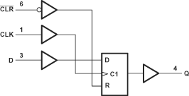
The SN74LVC1G175 device has an asynchronous clear (CLR) input. When CLR is high, data from the input pin (D) is transferred to the output pin (Q) on the clock's (CLK) rising edge. When CLR is low, Q is forced into the low state, regardless of the clock edge or data on D.
NanoFree™ package technology is a major breakthrough in IC packaging concepts, using the die as the package.
This device is fully specified for partial-power-down applications using Ioff. The Ioff circuitry disables the outputs, preventing damaging current backflow through the device when it is powered down.
8.2 Functional Block Diagram

8.3 Feature Description
The SN74LVC1G175 device has a wide operating VCC range of 1.65 V to 5.5 V, which allows it to be used in a broad range of systems. The 5.5-V I/Os allow down translation and also allow voltages at the inputs when
VCC = 0.
8.4 Device Functional Modes
Table 1 lists the functional modes for SN74LVC1G175.
Table 1. Function Table
| INPUTS | OUTPUT Q |
||
|---|---|---|---|
| CLR | CLK | D | |
| H | ↑ | L | L |
| H | ↑ | H | H |
| H | H or L | X | Q0 |
| L | X | X | L |