SCES648A February 2006 – August 2019 SN74LVC1G32-Q1
PRODUCTION DATA.
- 1 Features
- 2 Applications
- 3 Description
- 4 Revision History
- 5 Pin Configuration and Functions
-
6 Specifications
- 6.1 Absolute Maximum Ratings
- 6.2 ESD Ratings
- 6.3 Recommended Operating Conditions
- 6.4 Thermal Information
- 6.5 Electrical Characteristics
- 6.6 Switching Characteristics, CL = 15 pF
- 6.7 Switching Characteristics, 1.8 V and 2.5V
- 6.8 Switching Characteristics, 3.3 V and 5 V
- 6.9 Operating Characteristics
- 6.10 Typical Characteristics
- 7 Parameter Measurement Information
- 8 Detailed Description
- 9 Application and Implementation
- 10Power Supply Recommendations
- 11Layout
- 12Device and Documentation Support
- 13Mechanical, Packaging, and Orderable Information
Package Options
Mechanical Data (Package|Pins)
Thermal pad, mechanical data (Package|Pins)
- DRY|6
Orderable Information
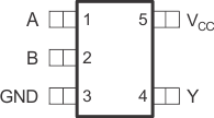
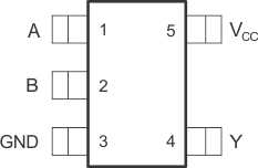
5 Pin Configuration and Functions
DCK package
5-Pin SC-70
(Top View)

DRY package
6-Pin SON
(Transparent Top View)

NC = No Connect
See Mechanical drawings at the end of the data sheet for dimensions
