SCES323Q June 2001 – March 2017 SN74LVC1G66
PRODUCTION DATA.
- 1 Features
- 2 Applications
- 3 Description
- 4 Revision History
- 5 Pin Configuration and Functions
- 6 Specifications
- 7 Parameter Measurement Information
- 8 Detailed Description
- 9 Application and Implementation
- 10Power Supply Recommendations
- 11Layout
- 12Device and Documentation Support
- 13Mechanical, Packaging, and Orderable Information
Package Options
Refer to the PDF data sheet for device specific package drawings
Mechanical Data (Package|Pins)
- DBV|5
- DSF|6
- DCK|5
- DRL|5
- DRY|6
- YZP|5
Thermal pad, mechanical data (Package|Pins)
- DRY|6
Orderable Information
7 Parameter Measurement Information
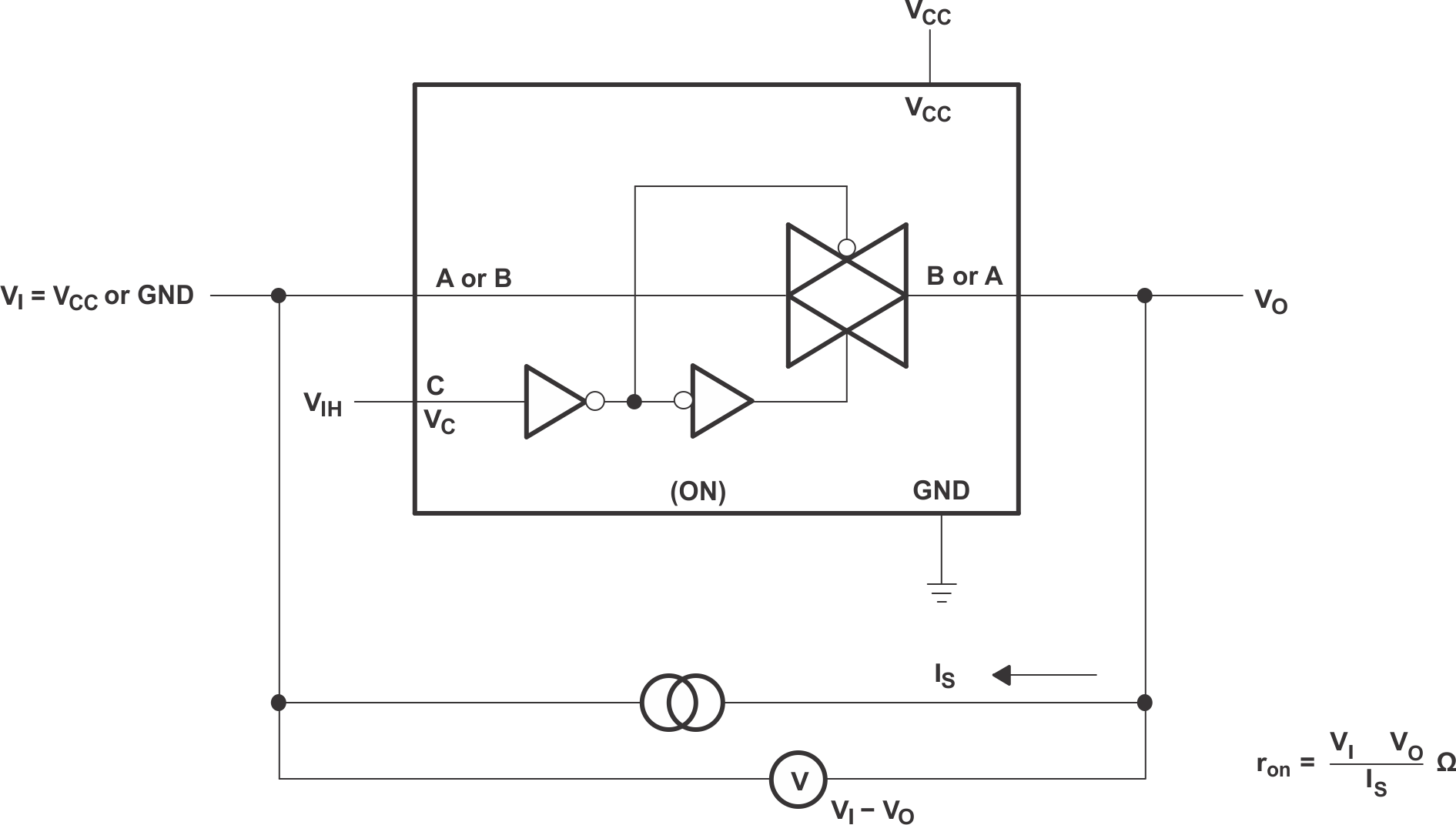 Figure 2. ON-State Resistance Test Circuit
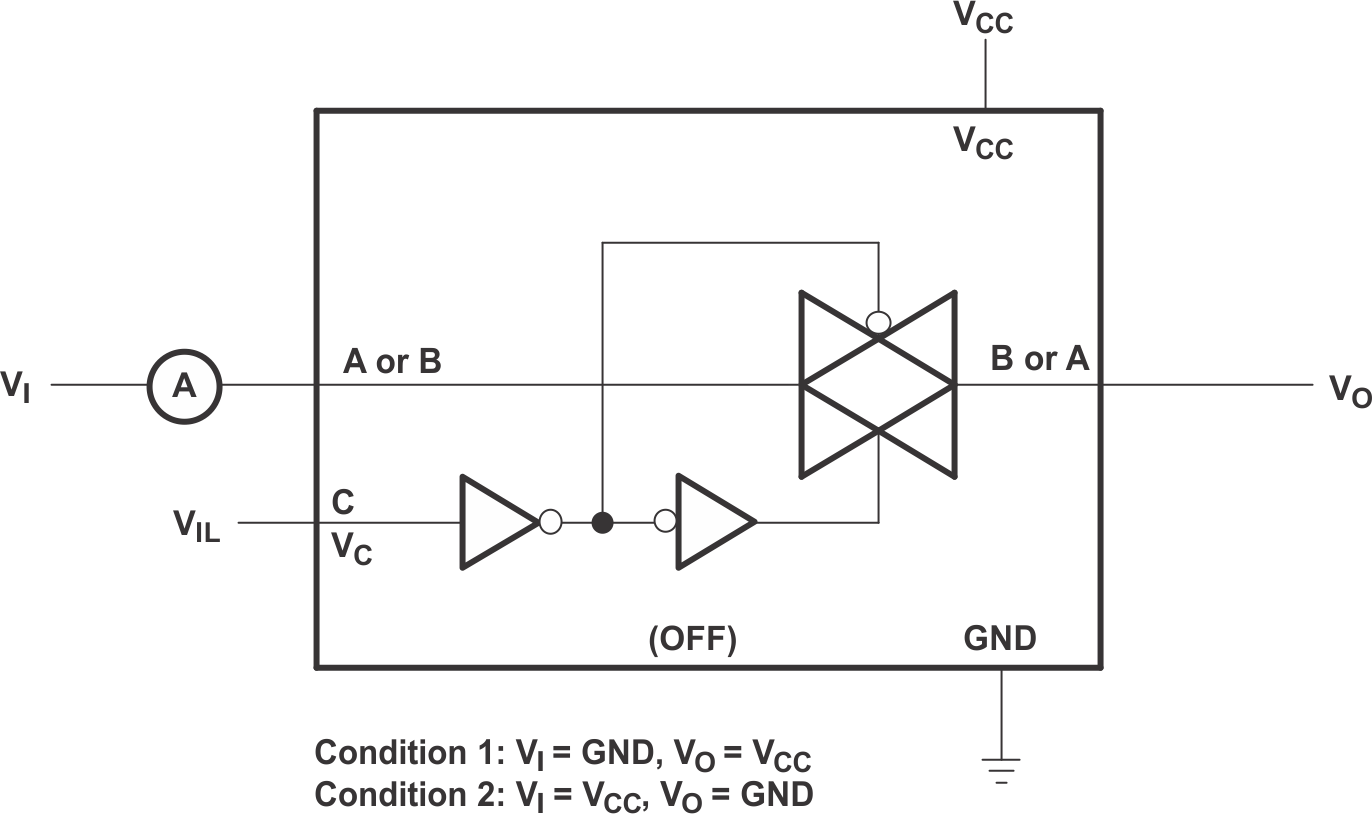 Figure 3. OFF-State Switch Leakage-Current Test Circuit
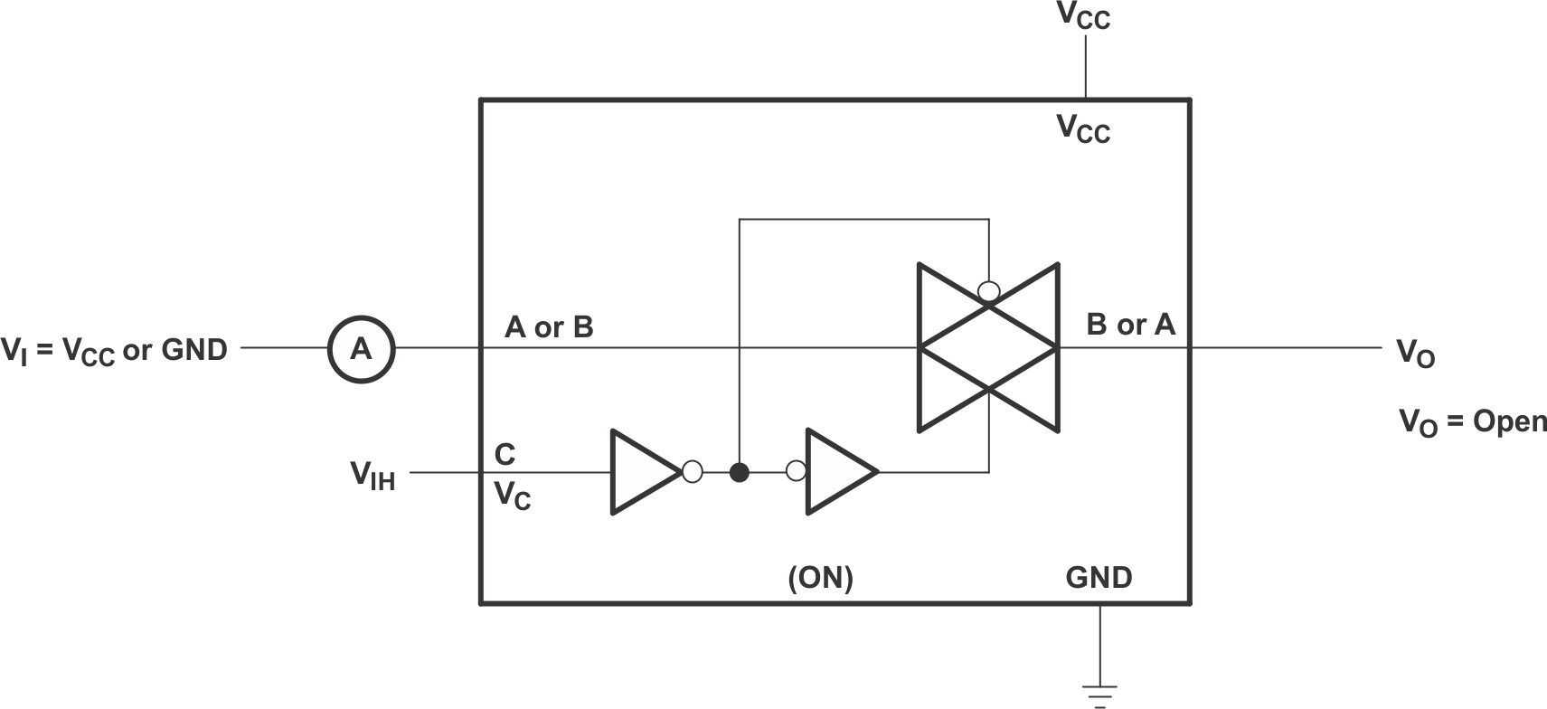 Figure 4. ON-State Switch Leakage-Current Test Circuit
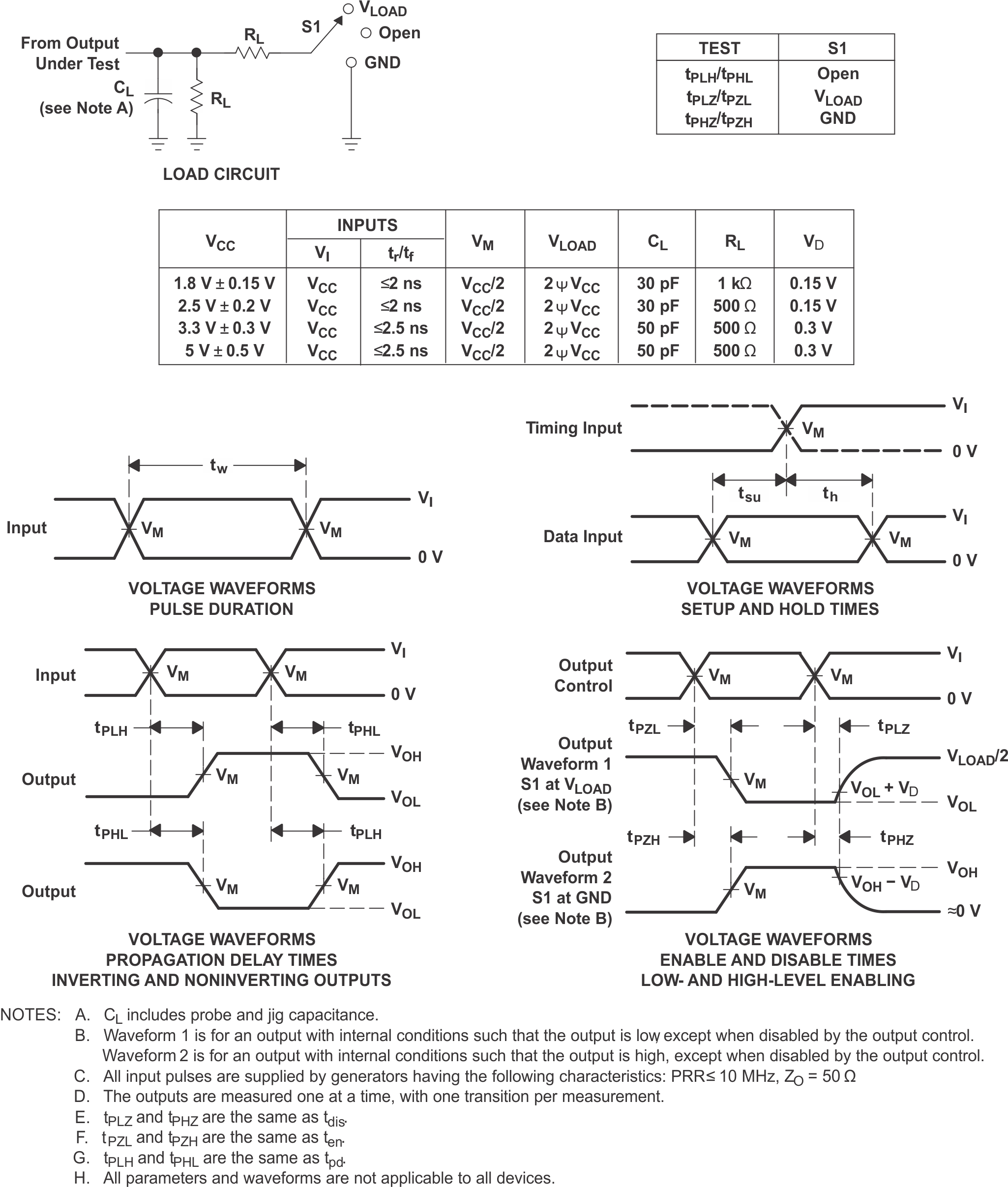 Figure 5. Load Circuit and Voltage Waveforms
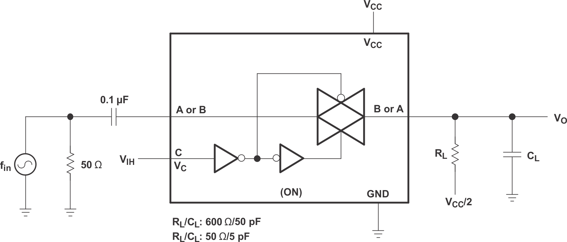 Figure 6. Frequency Response (Switch ON)
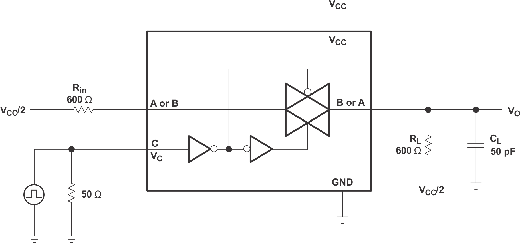 Figure 7. Crosstalk (Control Input – Switch Output)
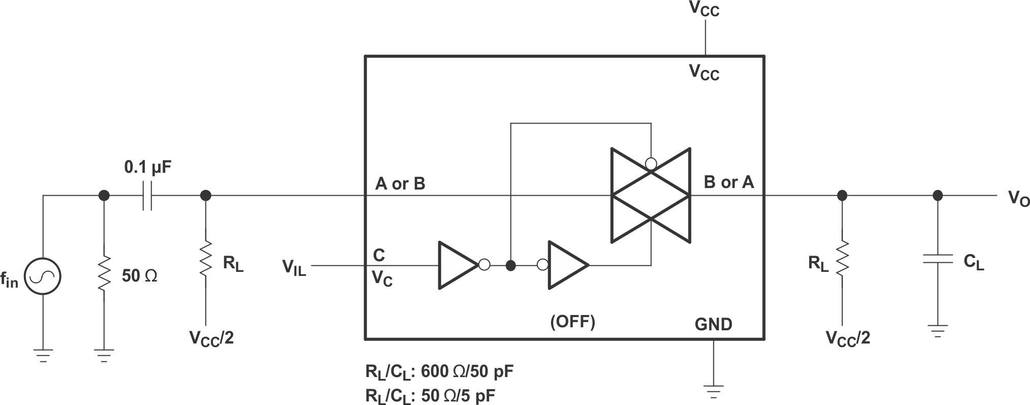 Figure 8. Feedthrough (Switch OFF)
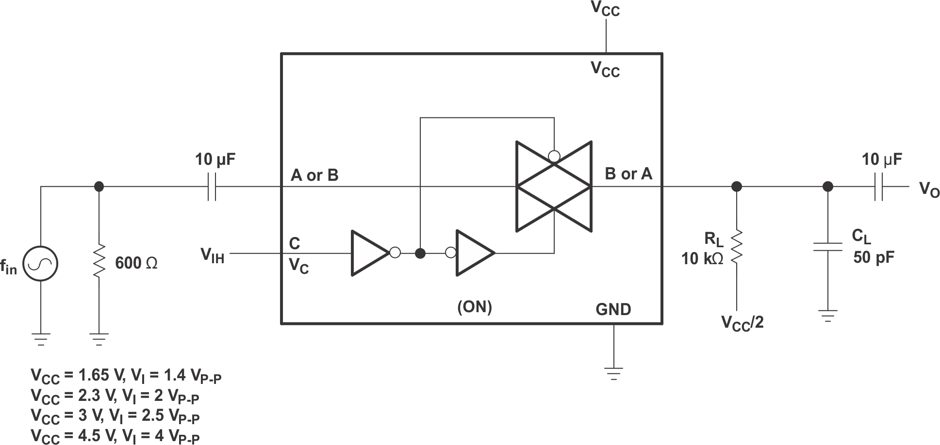 Figure 9. Sine-Wave Distortion