SCES581D JULY 2004 – October 2015 SN74LVC1GX04
UNLESS OTHERWISE NOTED, this document contains PRODUCTION DATA.
- 1 Features
- 2 Applications
- 3 Description
- 4 Revision History
- 5 Pin Configuration and Functions
-
6 Specifications
- 6.1 Absolute Maximum Ratings
- 6.2 ESD Ratings
- 6.3 Recommended Operating Conditions
- 6.4 Thermal Information
- 6.5 Electrical Characteristics
- 6.6 Switching Characteristics, SN74LVC1GX04
- 6.7 Switching Characteristics, SN74LVC1GX04
- 6.8 Switching Characteristics, SN74LVC1GX04
- 6.9 Operating Characteristics
- 6.10 Typical Characteristics
- 7 Parameter Measurement Information
- 8 Detailed Description
- 9 Application and Implementation
- 10Power Supply Recommendations
- 11Layout
- 12Device and Documentation Support
- 13Mechanical, Packaging, and Orderable Information
Package Options
Refer to the PDF data sheet for device specific package drawings
Mechanical Data (Package|Pins)
- DBV|6
- DRL|6
- DCK|6
Thermal pad, mechanical data (Package|Pins)
Orderable Information
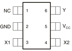
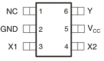
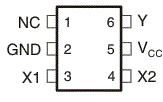
5 Pin Configuration and Functions
DBV Package
6-Pin SOT-23
Top View

DCK Package
6-Pin SC70
Top View

DRL Package
6-Pin SOT
Top View

See mechanical drawings for dimensions.
NC – No internal connection.
Pin Functions
| PIN | I/O | DESCRIPTION | |
|---|---|---|---|
| NAME | NO. | ||
| GND | 2 | – | Ground |
| NC | 1 | – | No internal connection |
| VCC | 5 | – | Supply power |
| X1 | 3 | I | Amplifier input |
| X2 | 4 | O | Amplifier output |
| Y | 6 | O | Main output to other logic |