SCES818C September 2010 – July 2024 SN74LVC2T45-Q1
PRODUCTION DATA
- 1
- 1 Features
- 2 Applications
- 3 Description
- 4 Pin Configuration and Functions
-
5 Specifications
- 5.1 Absolute Maximum Ratings
- 5.2 ESD Ratings
- 5.3 Recommended Operating Conditions
- 5.4 Thermal Information
- 5.5 Electrical Characteristics
- 5.6 Switching Characteristics: VCCA = 1.8V ± 0.15V
- 5.7 Switching Characteristics: VCCA = 2.5V ± 0.2V
- 5.8 Switching Characteristics: VCCA = 3.3V ± 0.3V
- 5.9 Switching Characteristics: VCCA = 5V ± 0.5V
- 5.10 Operating Characteristics
- 5.11 Typical Characteristics
- 6 Parameter Measurement Information
-
7 Detailed Description
- 7.1 Overview
- 7.2 Functional Block Diagram
- 7.3
Feature Description
- 7.3.1 Fully Configurable Dual-Rail Design Allows Each Port to Operate Over the Full 1.65V to 5.5V Power-Supply Range
- 7.3.2 Support High-Speed Translation
- 7.3.3 Ioff Supports Partial-Power-Down Mode Operation
- 7.3.4 Balanced High-Drive CMOS Push-Pull Outputs
- 7.3.5 Glitch-Free Power Supply Sequencing
- 7.3.6 Vcc Isolation
- 7.4 Device Functional Modes
- 8 Application and Implementation
- 9 Device and Documentation Support
- 10Revision History
- 11Mechanical, Packaging, and Orderable Information
Refer to the PDF data sheet for device specific package drawings
Mechanical Data (Package|Pins)
- DCU|8
Thermal pad, mechanical data (Package|Pins)
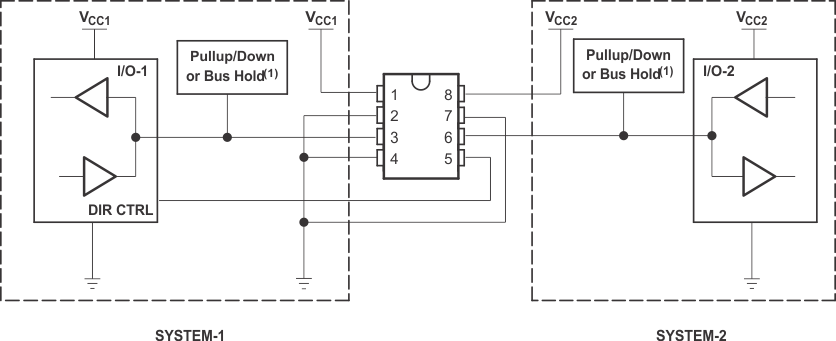
8.2.2 Bidirectional Logic Level-Shifting Application
Figure 8-2 shows the SN74LVC2T45-Q1 being used in a bidirectional logic level-shifting application. Because the SN74LVC2T45-Q1 does not have an output-enable (OE) pin, the system designer should take precautions to avoid bus contention between SYSTEM-1 and SYSTEM-2 when changing directions.
 Figure 8-2 Bidirectional Logic Level-Shifting Application