SCAS288R January 1993 – August 2024 SN54LVC86A , SN74LVC86A
PRODUCTION DATA
- 1
- 1 Features
- 2 Applications
- 3 Description
- 4 Pin Configuration and Functions
-
5 Specifications
- 5.1 Absolute Maximum Ratings
- 5.2 ESD Ratings
- 5.3 Recommended Operating Conditions, SN54LVC86A
- 5.4 Recommended Operating Conditions, SN74LVC86A
- 5.5 Thermal Information
- 5.6 Electrical Characteristics, SN54LVC86A
- 5.7 Electrical Characteristics, SN74LVC86A
- 5.8 Switching Characteristics, SN54LVC86A
- 5.9 Switching Characteristics, SN74LVC86A
- 5.10 Operating Characteristics
- 5.11 Typical Characteristics
- 6 Parameter Measurement Information
- 7 Detailed Description
- 8 Application and Implementation
- 9 Device and Documentation Support
- 10Revision History
- 11Mechanical, Packaging, and Orderable Information
Package Options
Refer to the PDF data sheet for device specific package drawings
Mechanical Data (Package|Pins)
- D|14
- RGY|14
- DB|14
- PW|14
- BQA|14
- NS|14
Thermal pad, mechanical data (Package|Pins)
Orderable Information
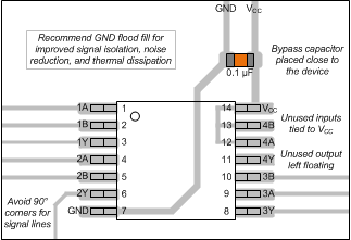
8.3.2 Layout Example
 Figure 8-3 Example
Layout for the SN74LVC86A