SCAS568N March 1996 – September 2014 SN74LVCH16373A
PRODUCTION DATA.
- 1 Features
- 2 Applications
- 3 Description
- 4 Simplified Schematic
- 5 Revision History
- 6 Pin Configuration and Functions
-
7 Specifications
- 7.1 Absolute Maximum Ratings
- 7.2 Handling Ratings
- 7.3 Recommended Operating Conditions
- 7.4 Thermal Information
- 7.5 Electrical Characteristics
- 7.6 Timing Requirements, -40°C to 85°C
- 7.7 Timing Requirements, -40°C to 125°C
- 7.8 Switching Characteristics, -40°C to 85°C
- 7.9 Switching Characteristics, -40°C to 125°C
- 7.10 Operating Characteristics
- 7.11 Typical Characteristics
- 8 Parameter Measurement Information
- 9 Detailed Description
- 10Application and Implementation
- 11Power Supply Recommendations
- 12Layout
- 13Device and Documentation Support
- 14Mechanical, Packaging, and Orderable Information
Package Options
Refer to the PDF data sheet for device specific package drawings
Mechanical Data (Package|Pins)
- DGG|48
- DL|48
- DGV|48
Thermal pad, mechanical data (Package|Pins)
Orderable Information
10 Application and Implementation
NOTE
Information in the following applications sections is not part of the TI component specification, and TI does not warrant its accuracy or completeness. TI’s customers are responsible for determining suitability of components for their purposes. Customers should validate and test their design implementation to confirm system functionality.
10.1 Application Information
The SN74LVCH16373A is a high-drive CMOS device that can be used for a multitude of bus interface type applications where the data needs to be retained or latched. It can produce 24 mA of drive current at 3.3 V; therefore making it ideal for driving multiple outputs. This device is also good for high-speed applications up to 100 MHz. The inputs are 5.5-V tolerant allowing translation down to VCC.
10.2 Typical Application
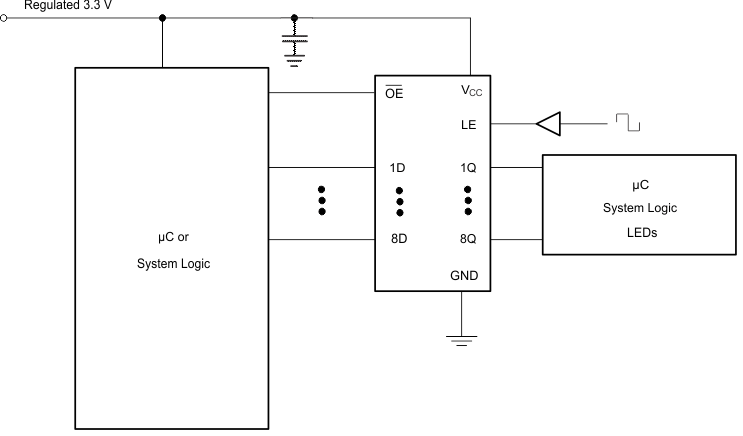 Figure 5. Typical Application Schematic
10.2.1 Design Requirements
This device uses CMOS technology and has balanced output drive. Care should be taken to avoid bus contention because it can drive currents that would exceed maximum limits. The high drive will also create fast edges into light loads; therefore, routing and load conditions should be considered to prevent ringing.
10.2.2 Detailed Design Procedure
- Recommended input conditions
- Rise time and fall time specs: See (Δt/ΔV) in the Recommended Operating Conditions table.
- Specified High and low levels: See (VIH and VIL) in the Recommended Operating Conditions table.
- Inputs are overvoltage tolerant allowing them to go as high as 5.5 V at any valid VCC.
- Recommend output conditions
- Load currents should not exceed 50 mA per output and 100 mA total for the part.
- Outputs should not be pulled above VCC.
10.2.3 Application Curves
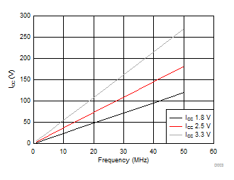 Figure 6. ICC vs Frequency