SCAS319J November 1993 – December 2014 SN74LVCH16652A
PRODUCTION DATA.
- 1 Features
- 2 Applications
- 3 Description
- 4 Simplified Schematic
- 5 Revision History
- 6 Pin Configuration and Functions
-
7 Specifications
- 7.1 Absolute Maximum Ratings
- 7.2 ESD Ratings
- 7.3 Recommended Operating Conditions
- 7.4 Thermal Information
- 7.5 Electrical Characteristics
- 7.6 Timing Requirements, 40°C to 85°C
- 7.7 Timing Requirements, 40°C to 125°C
- 7.8 Switching Characteristics, 40°C to 85°C
- 7.9 Switching Characteristics, 40°C to 125°C
- 7.10 Operating Characteristics
- 7.11 Typical Characteristics
- 8 Parameter Measurement Information
- 9 Detailed Description
- 10Application and Implementation
- 11Power Supply Recommendations
- 12Layout
- 13Device and Documentation Support
- 14Mechanical, Packaging, and Orderable Information
Package Options
Refer to the PDF data sheet for device specific package drawings
Mechanical Data (Package|Pins)
- DGG|56
- DL|56
- DGV|56
Thermal pad, mechanical data (Package|Pins)
Orderable Information
9 Detailed Description
9.1 Overview
This 16-bit bus transceiver and register is designed for 1.65-V to 3.6-V VCC operation.
The SN74LVCH16652A device consists of D-type flip-flops and control circuitry arranged for multiplexed transmission of data directly from the data bus or from the internal storage registers. The device can be used as two 8-bit transceivers or one 16-bit transceiver.
Complementary output-enable (OEAB and OEBA) inputs control the transceiver functions. Select-control (SAB and SBA) inputs select whether real-time or stored data is transferred. A low input level selects real-time data, and a high input level selects stored data. The circuitry used for select control eliminates the typical decoding glitch that occurs in a multiplexer during the transition between stored and real-time data. Figure 5 illustrates the four fundamental bus-management functions that can be performed with SN74LVCH16652A.
Data on the A or B bus, or both, can be stored in the internal D flip-flops by low-to-high transitions at the appropriate clock (CLKAB or CLKBA) inputs, regardless of the levels on the select-control or output-enable inputs. When SAB and SBA are in the real-time transfer mode, it also is possible to store data without using the internal D-type flip-flops by simultaneously enabling OEAB and OEBA. In this configuration, each output reinforces its input. When all other data sources to the two sets of bus lines are at high impedance, each set of bus lines remains at its last level configuration.
To ensure the high-impedance state during power up or power down, OEBA should be tied to VCC through a pull-up resistor and OEAB should be tied to GND through a pull-down resistor; the minimum value of the resistor is determined by the current-sinking/current-sourcing capability of the driver.
Inputs can be driven from either 3.3-V or 5-V devices. This feature allows the use of these devices as translators in a mixed 3.3-V/5-V system environment.
Active bus-hold circuitry is provided to hold unused or floating data inputs at a valid logic level. Use of pull-up or pull-down resistors with the bus-hold circuitry is not recommended. The bus-hold circuitry is part of the input circuit and is not disabled by OE or DIR.
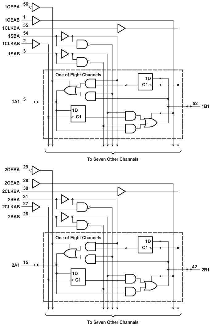
9.2 Functional Block Diagram
 Figure 4. Logic Diagram (Positive Logic)
9.3 Feature Description
- Wide operating voltage range
- Operates from 1.65 V to 3.6 V
- Allows down voltage translation
- Inputs accept voltages to 5.5 V
- Ioff feature
- Allows voltages on the inputs and outputs when VCC is 0 V
- Bus hold on data Inputs eliminates the need for external pull-up/pull-down resistors
9.4 Device Functional Modes
Table 1. Function Table
| INPUTS | DATA I/O(1) | OPERATION OR FUNCTION | ||||||
|---|---|---|---|---|---|---|---|---|
| OEAB | OEBA | CLKAB | CLKBA | SAB | SBA | A1–A8 | B1–B8 | |
| L | H | H or L | H or L | X | X | Input | Input | Isolation |
| L | H | ↑ | ↑ | X | X | Input | Input | Store A and B data |
| X | H | ↑ | H or L | X | X | Input | Unspecified(2) | Store A, hold B |
| H | H | ↑ | ↑ | X(2) | X | Input | Output | Store A in both registers |
| L | X | H or L | ↑ | X | X | Unspecified(2) | Input | Hold A, store B |
| L | L | ↑ | ↑ | X | X(2) | Output | Input | Store B in both registers |
| L | L | X | X | X | L | Output | Input | Real-time B data to A bus |
| L | L | X | H or L | X | H | Output | Input | Stored B data to A bus |
| H | H | X | X | L | X | Input | Output | Real-time A data to B bus |
| H | H | H or L | X | H | X | Input | Output | Stored A data to B bus |
| H | L | H or L | H or L | H | H | Output | Output | Stored A data to B bus and stored B data to A bus |
Select control = H; clocks must be staggered to load both registers.