SCES950 August 2022 SN74LXC1T14-Q1
PRODUCTION DATA
- 1 Features
- 2 Applications
- 3 Description
- 4 Revision History
- 5 Pin Configuration and Functions
- 6 Specifications
- 7 Parameter Measurement Information
-
8 Detailed Description
- 8.1 Overview
- 8.2 Functional Block Diagram
- 8.3
Feature Description
- 8.3.1 CMOS Schmitt-Trigger Inputs with Integrated Pulldowns
- 8.3.2 Balanced High-Drive CMOS Push-Pull Outputs
- 8.3.3 Partial Power Down (Ioff)
- 8.3.4 VCC Isolation and VCC Disconnect (Ioff-float)
- 8.3.5 Over-Voltage Tolerant Inputs
- 8.3.6 Glitch-Free Power Supply Sequencing
- 8.3.7 Negative Clamping Diodes
- 8.3.8 Fully Configurable Dual-Rail Design
- 8.3.9 Supports High-Speed Translation
- 8.4 Device Functional Modes
- 9 Application and Implementation
- 10Power Supply Recommendations
- 11Layout
- 12Device and Documentation Support
- 13Mechanical, Packaging, and Orderable Information
Package Options
Mechanical Data (Package|Pins)
- DCK|5
Thermal pad, mechanical data (Package|Pins)
Orderable Information
6.8 Typical Characteristics
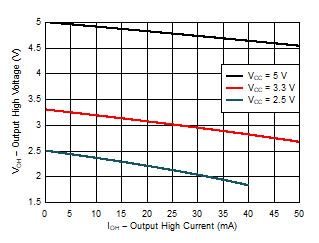 Figure 6-1 Typical (TA=25°C) Output
High Voltage (VOH) vs Source Current (IOH)
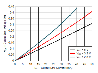 Figure 6-3 Typical (TA=25°C) Output
High Voltage (VOL) vs Sink Current (IOL)
 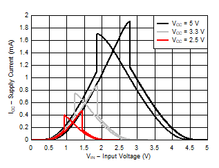 Figure 6-5 Typical (TA=25°C) Supply
Current (ICC) vs Input Voltage (VIN)
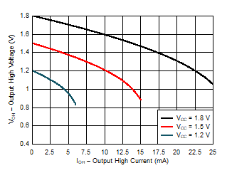 Figure 6-2 Typical (TA=25°C) Output
High Voltage (VOH) vs Source Current (IOH)
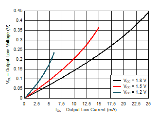 Figure 6-4 Typical (TA=25°C) Output
High Voltage (VOL) vs Sink Current (IOL)
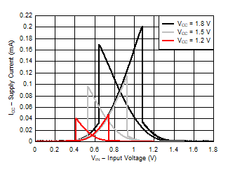 Figure 6-6 Typical (TA=25°C) Supply
Current (ICC) vs Input Voltage (VIN)