SCES938B October 2021 – May 2022 SN74LXC2T45
PRODUCTION DATA
- 1 Features
- 2 Applications
- 3 Description
- 4 Revision History
- 5 Pin Configuration and Functions
-
6 Specifications
- 6.1 Absolute Maximum Ratings
- 6.2 ESD Ratings
- 6.3 Recommended Operating Conditions
- 6.4 Thermal Information
- 6.5 Electrical Characteristics
- 6.6 Switching Characteristics: Tsk, TMAX
- 6.7 Switching Characteristics, VCCA = 1.2 ± 0.1 V
- 6.8 Switching Characteristics, VCCA = 1.5 ± 0.1 V
- 6.9 Switching Characteristics, VCCA = 1.8 ± 0.15 V
- 6.10 Switching Characteristics, VCCA = 2.5 ± 0.2 V
- 6.11 Switching Characteristics, VCCA = 3.3 ± 0.3 V
- 6.12 Switching Characteristics, VCCA = 5.0 ± 0.5 V
- 6.13 Operating Characteristics
- 6.14 Typical Characteristics
- 7 Parameter Measurement Information
- 8 Detailed Description
- 9 Partial Power Down (Ioff)
- 10VCC Isolation and VCC Disconnect (Ioff-float)
- 11Over-Voltage Tolerant Inputs
- 12Glitch-Free Power Supply Sequencing
- 13Negative Clamping Diodes
- 14Fully Configurable Dual-Rail Design
- 15Supports High-Speed Translation
- 16Device Functional Modes
- 17Application and Implementation
- 18Power Supply Recommendations
- 19Layout
- 20Device and Documentation Support
- 21Mechanical, Packaging, and Orderable Information
Package Options
Mechanical Data (Package|Pins)
Thermal pad, mechanical data (Package|Pins)
Orderable Information
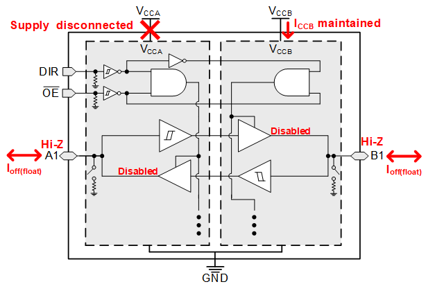
10 VCC Isolation and VCC Disconnect (Ioff-float)
This device has I/O's with Integrated Pull-Down Resistors. The I/O's will get pulled down and then enter a high-impedance state when either supply is < 100 mV or left floating (disconnected), while the other supply is still connected to the device. It is recommended that the I/O's for this device are not driven and kept at a logic low state prior to floating (disconnecting) either supply.
The maximum supply current is specified by ICCx, while VCCx is floating, in the Electrical Characterstics. The maximum leakage into or out of any input or output pin on the device is specified by Ioff(float) in the Electrical Characteristics.
 Figure 10-1 VCC Disconnect
Feature