SLRS021D December 1967 – January 2017 SN55451B , SN55452B , SN55453B , SN55454B , SN75451B , SN75452B , SN75453B , SN75454B
PRODUCTION DATA.
- 1 Features
- 2 Applications
- 3 Description
- 4 Revision History
- 5 Device Comparison Table
- 6 Pin Configuration and Functions
- 7 Specifications
- 8 Parameter Measurement Information
- 9 Detailed Description
- 10Application and Implementation
- 11Power Supply Recommendations
- 12Layout
- 13Device and Documentation Support
- 14Mechanical, Packaging, and Orderable Information
Package Options
Refer to the PDF data sheet for device specific package drawings
Mechanical Data (Package|Pins)
- D|8
- P|8
- PS|8
Thermal pad, mechanical data (Package|Pins)
- PS|8
Orderable Information
6 Pin Configuration and Functions
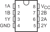
JG, D, P, or PS Package
8-Pin CDIP, SOIC, PDIP, or SO
Top View

FK Package
20-Pin LCCC
Top View

Pin Functions
| PIN | I/O | DESCRIPTION | ||
|---|---|---|---|---|
| NAME | CDIP, SOIC, PDIP, SO | LCCC | ||
| 1A | 1 | 2 | I | Channel 1 Logic Input A |
| 1B | 2 | 5 | I | Channel 1 Logic Input B |
| 1Y | 3 | 7 | O | Channel 1 Driver |
| 2A | 6 | 15 | I | Channel 2 Logic Input A |
| 2B | 7 | 17 | I | Channel 2 Logic Input B |
| 2Y | 5 | 12 | O | Channel 2 Driver |
| GND | 4 | 10 | — | Ground |
| NC | — | 1, 3, 4, 6, 8, 9, 11, 13, 14, 16, 18, 19 | — | No Internal Connection |
| VCC | 8 | 20 | — | Supply Voltage |