SLRS023E December 1976 – January 2015 SN75468 , SN75469
PRODUCTION DATA.
- 1 Features
- 2 Applications
- 3 Description
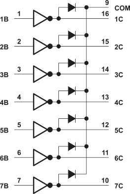
- 4 Simplified Schematic
- 5 Revision History
- 6 Pin Configuration and Functions
- 7 Specifications
- 8 Parameter Measurement Information
- 9 Detailed Description
- 10Application and Implementation
- 11Power Supply Recommendations
- 12Layout
- 13Device and Documentation Support
- 14Mechanical, Packaging, and Orderable Information
Package Options
Refer to the PDF data sheet for device specific package drawings
Mechanical Data (Package|Pins)
- N|16
- D|16
Thermal pad, mechanical data (Package|Pins)
Orderable Information
1 Features
2 Applications
- Relay Drivers
- Hammer Drivers
- Lamp Drivers
- Display Drivers (LED and Gas Discharge)
- Line Drivers
- Logic Buffers
3 Description
The SN75468 and SN75469 are high-voltage, high-current Darlington transistor arrays. Each consists of seven NPN Darlington pairs that feature high-voltage outputs with common-cathode clamp diodes for switching inductive loads. The collector-current rating of each Darlington pair is 500 mA. The Darlington pairs may be paralleled for higher current capability. Applications include relay drivers, hammer drivers, lamp drivers, display drivers (LED and gas discharge), line drivers, and logic buffers.
The SN75468 has a 2700-Ω series base resistor for each Darlington pair for operation directly with TTL or 5-V CMOS. The SN75469 has a 10.5-kΩ series base resistor to allow its operation directly with CMOS or PMOS that use supply voltages of 6 to 15 V. The required input current is below that of the SN75468.
Device Information(1)
| PART NUMBER | PACKAGE (PIN) | BODY SIZE (NOM) |
|---|---|---|
| SN7546x | D (16) | 9.90 mm × 3.91 mm |
| N (16) | 19.30 mm × 6.35 mm | |
| NS (16) | 10.30 mm × 5.30 mm |
- For all available packages, see the orderable addendum at the end of the datasheet.
4 Simplified Schematic