SLLS131D September 1991 – October 2023 SN75ALS175
PRODUCTION DATA
- 1
- 1 Features
- 2 Applications
- 3 Description
- 4 Pin Configuration and Functions
- 5 Specifications
- 6 Parameter Measurement Information
- 7 Detailed Description
- 8 Device and Documentation Support
- 9 Revision History
- 10Mechanical, Packaging, and Orderable Information
Package Options
Refer to the PDF data sheet for device specific package drawings
Mechanical Data (Package|Pins)
- NS|16
- N|16
Thermal pad, mechanical data (Package|Pins)
Orderable Information
6 Parameter Measurement Information
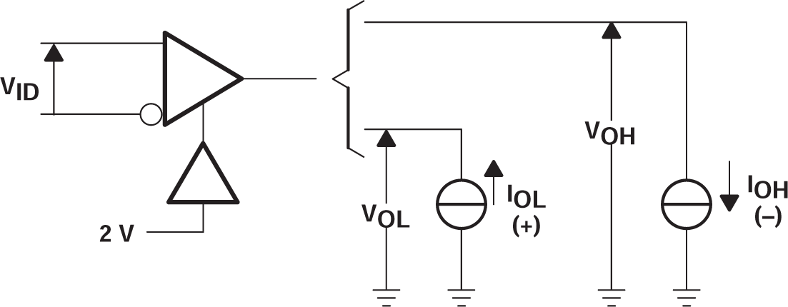
 Figure 6-1 VOH, VOL

A. The input pulse is supplied by a generator having the following characteristics: PRR = 1 MHz, duty cycle = 50%, tr = tf = 6 ns.
B. CL includes probe and jig capacitance.
Figure 6-2 Propagation Delay Times
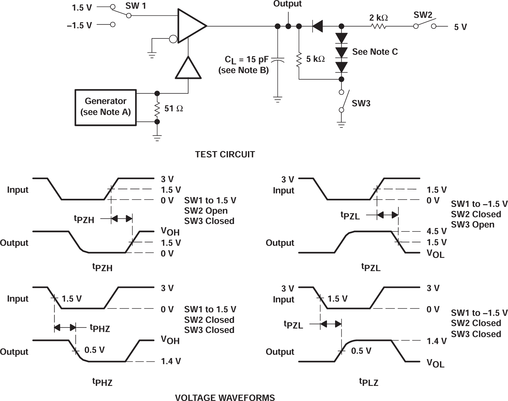
A. The input pulse is supplied by a generator having the following characteristics: PRR = 1 MHz, duty cycle = 50%, tr = tf = 6 ns.
B. CL includes probe and jig capacitance.
C. All diodes are 1N916 or equivalent.
Figure 6-3 Enable and Disable Times