SLLS032C December 1987 – March 2024 SN75ALS191
PRODUCTION DATA
- 1
- 1 Features
- 2 Applications
- 3 Description
- 4 Pin Configuration and Functions
- 5 Specifications
- 6 Parameter Measurement Information
- 7 Detailed Description
- 8 Device and Documentation Support
- 9 Revision History
- 10Mechanical, Packaging, and Orderable Information
Package Options
Refer to the PDF data sheet for device specific package drawings
Mechanical Data (Package|Pins)
- D|8
- P|8
- PS|8
Thermal pad, mechanical data (Package|Pins)
- PS|8
Orderable Information
7.1 Device Functional Modes
Table 7-1 Function Table (Each Driver)
| INPUTS A(1) | OUTPUTS | |
|---|---|---|
| Y | Z | |
| H | H | L |
| L | L | H |
(1) H = high level, L = low level, Z = high impedance
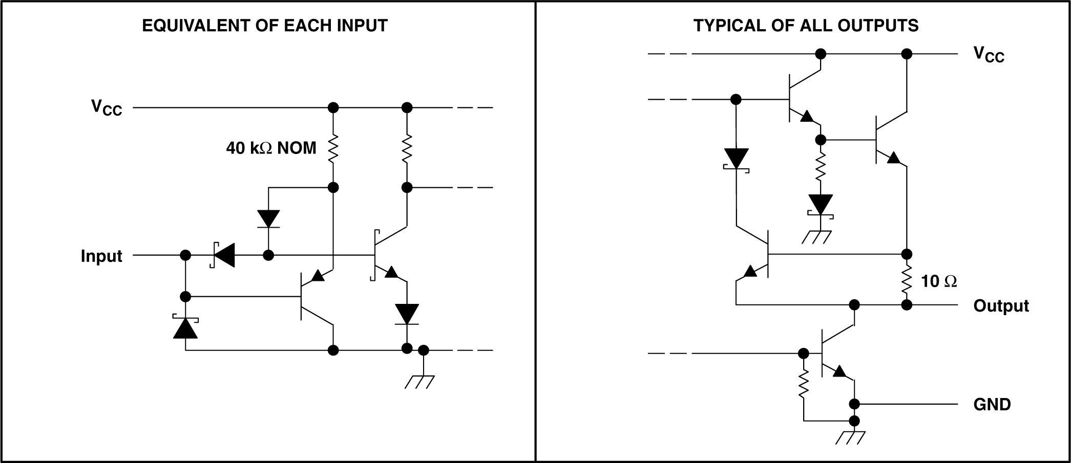
 Figure 7-1 Schematics of Inputs and
Outputs