SLLS045C January 1989 – October 2023 SN75ALS197
PRODUCTION DATA
- 1
- 1 Features
- 2 Applications
- 3 Description
- 4 Pin Configuration and Functions
- 5 Specifications
- 6 Parameter Measurement Information
- 7 Detailed Description
- 8 Device and Documentation Support
- 9 Revision History
- 10Mechanical, Packaging, and Orderable Information
Package Options
Refer to the PDF data sheet for device specific package drawings
Mechanical Data (Package|Pins)
- NS|16
- N|16
- D|16
Thermal pad, mechanical data (Package|Pins)
Orderable Information
5.7 Typical Characteristics
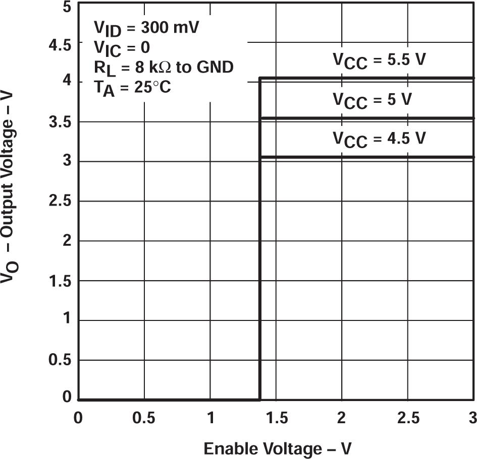 Figure 5-1 Output Voltage vs Enable
Voltage
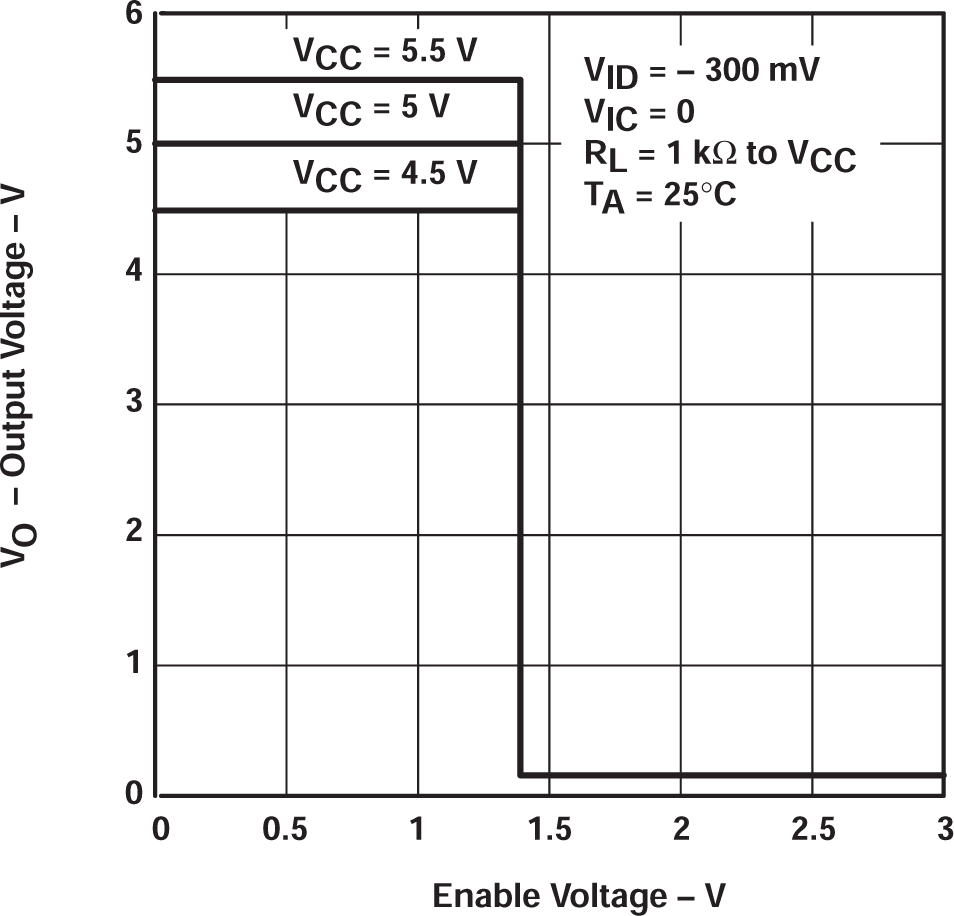 Figure 5-3 Output Voltage vs Enable
Voltage
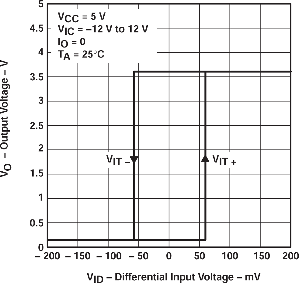 Figure 5-5 Output Voltage vs
Differential Input Voltage
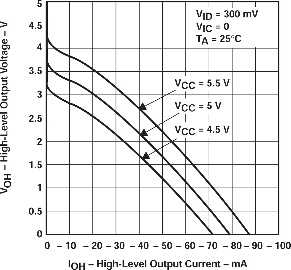 Figure 5-7 High-level Output Voltage
vs High-level Output Current
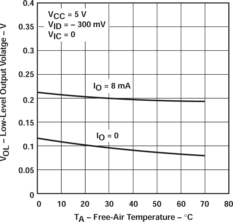 Figure 5-9 Low-level Output Voltage
vs Free-air Temperature
 Figure 5-11 Low-level Output Voltage
vs Low-level Output Current
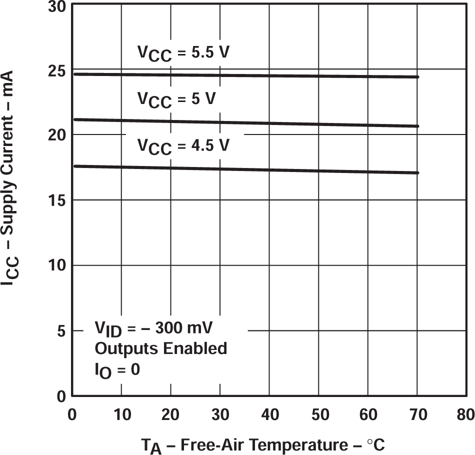 Figure 5-13 Supply Current vs Free-air
Temperature
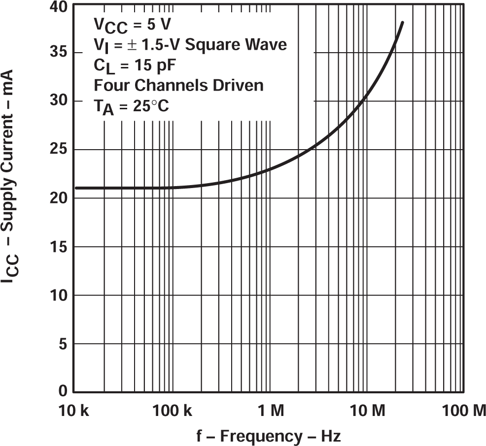 Figure 5-15 Supply Current vs
Frequency
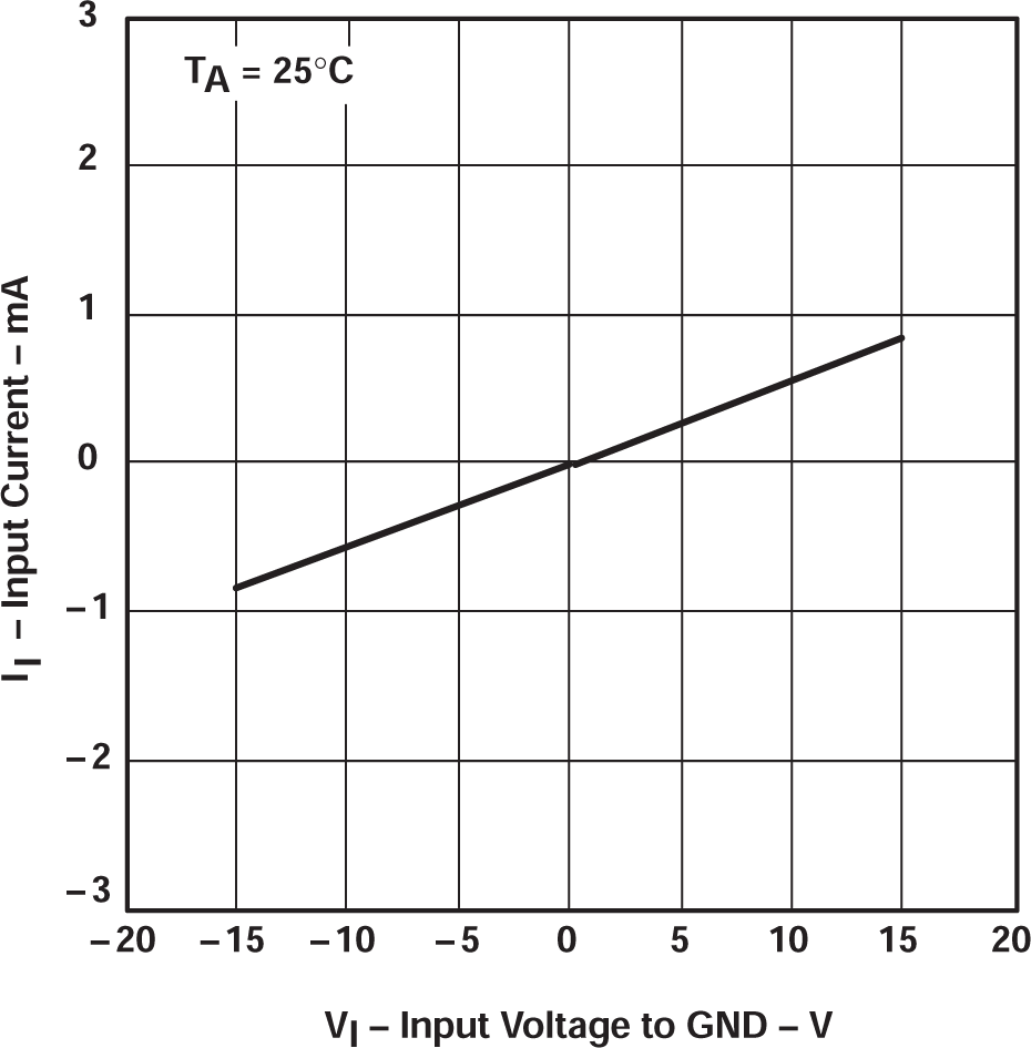 Figure 5-17 Input Current vs Input
Voltage to Gnd
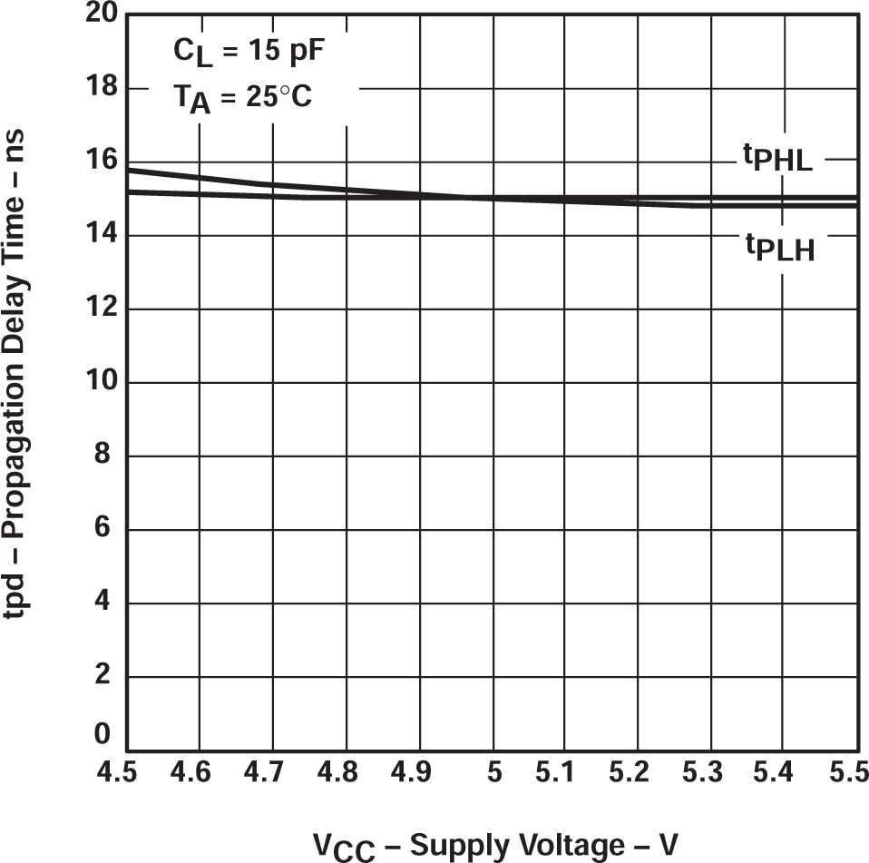 Figure 5-19 Propagation Delay Time vs
Supply Voltage
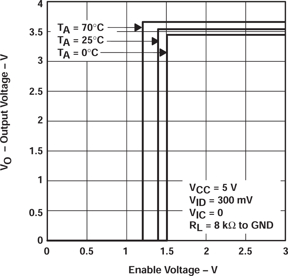 Figure 5-2 Output Voltage vs Enable
Voltage
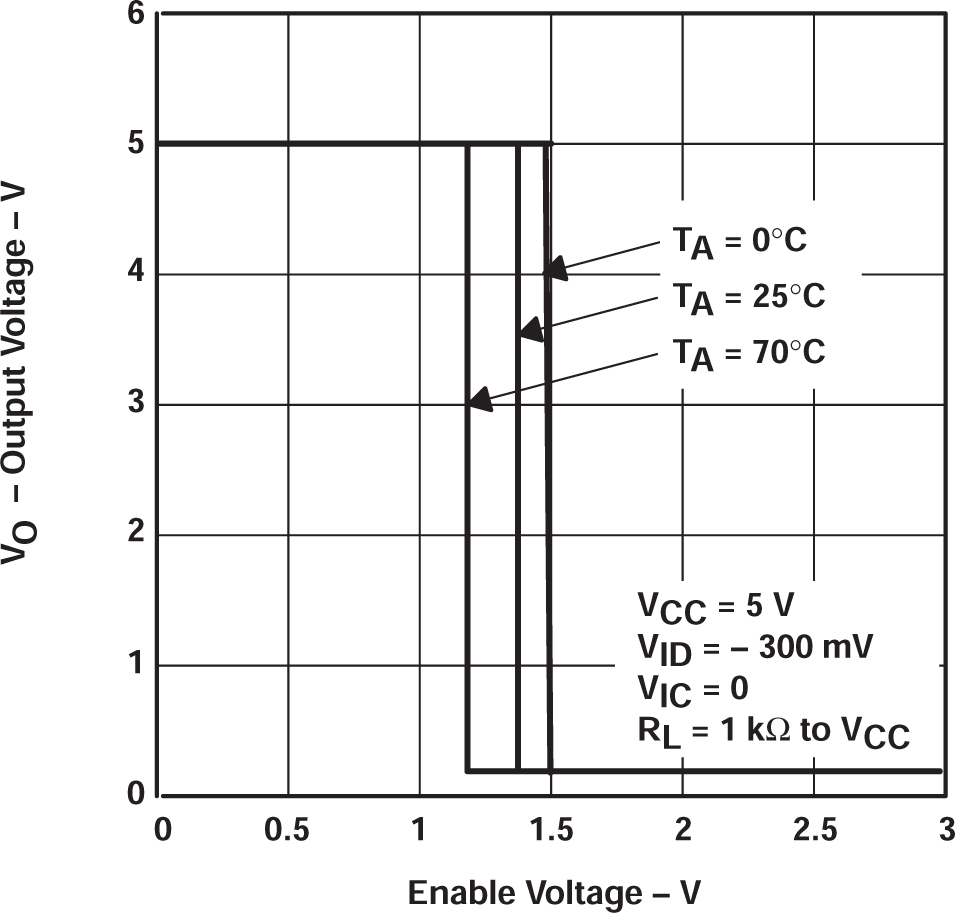 Figure 5-4 Output Voltage vs Enable
Voltage
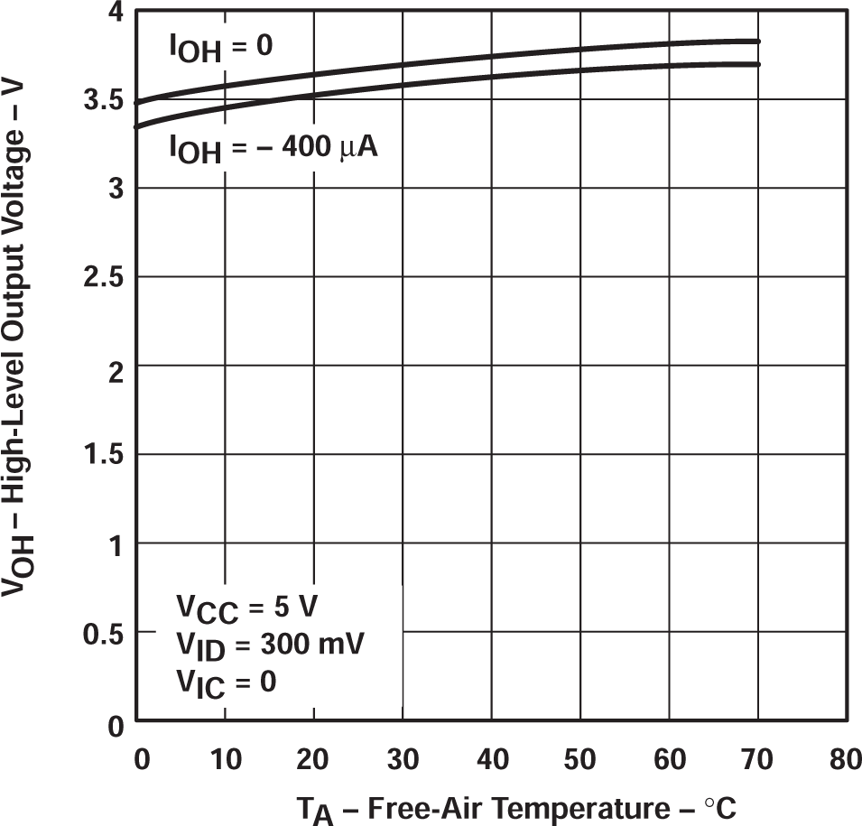 Figure 5-6 High-level Output Voltage
vs Free-air Temperature
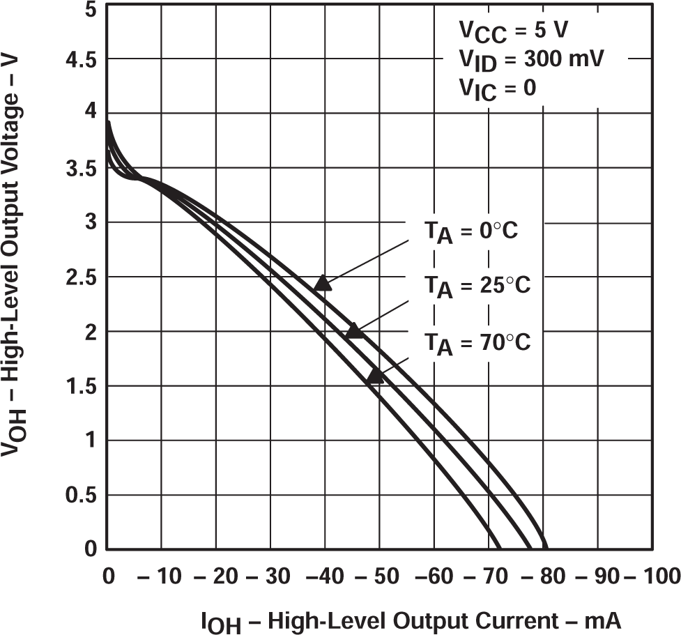 Figure 5-8 High-level Output Voltage
vs High-level Output Current
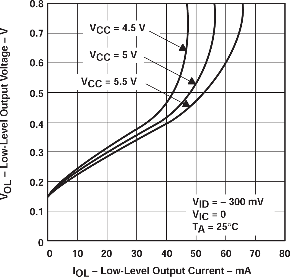 Figure 5-10 Low-level Output Voltage
vs Low-level Output Current
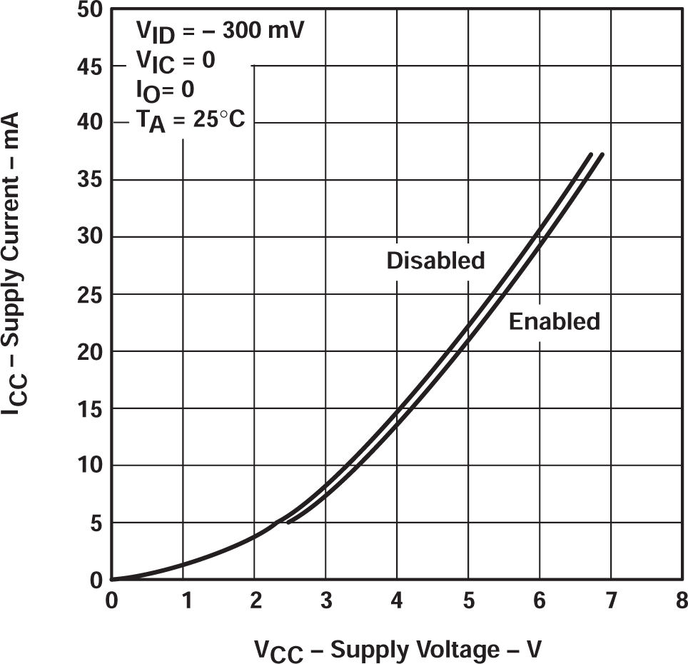 Figure 5-12 Supply Current vs Supply
Voltage
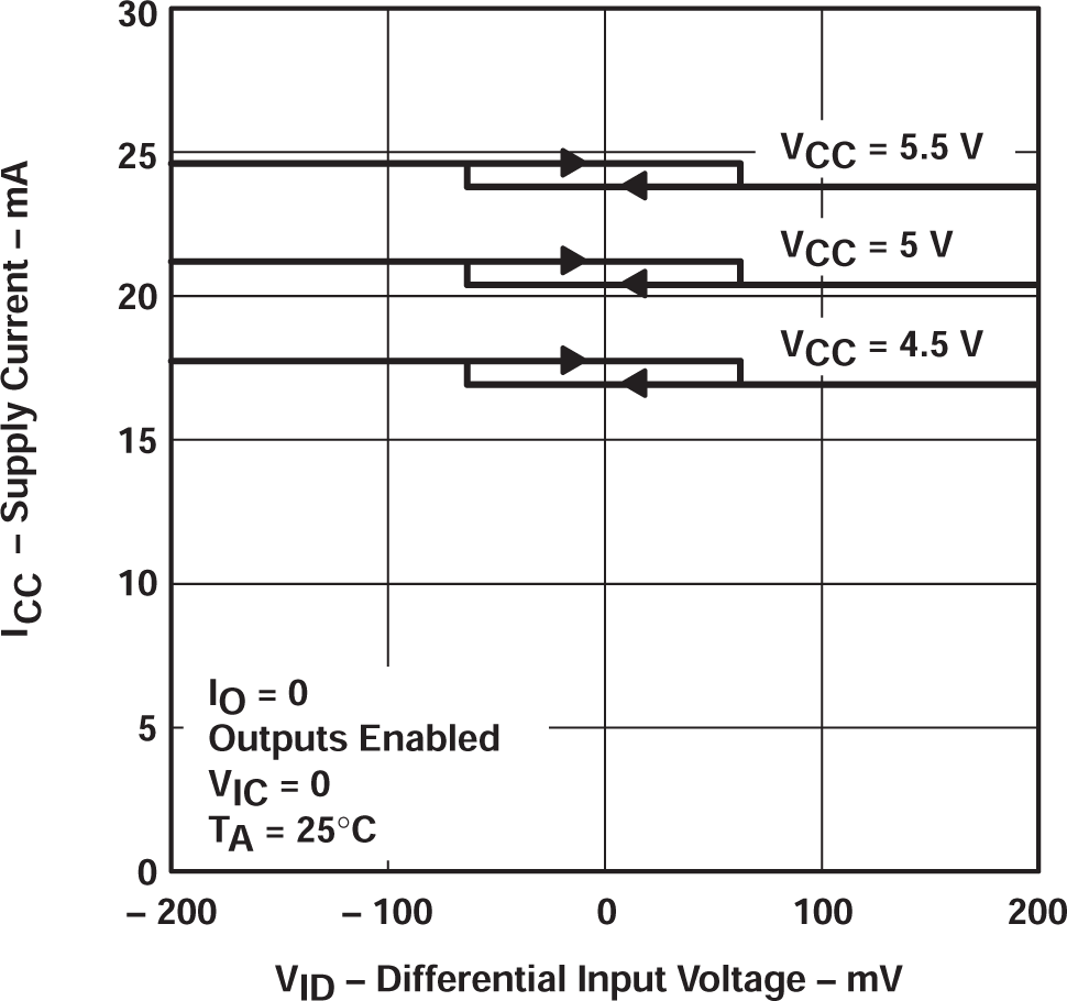 Figure 5-14 Supply Current vs
Differential Input Voltage
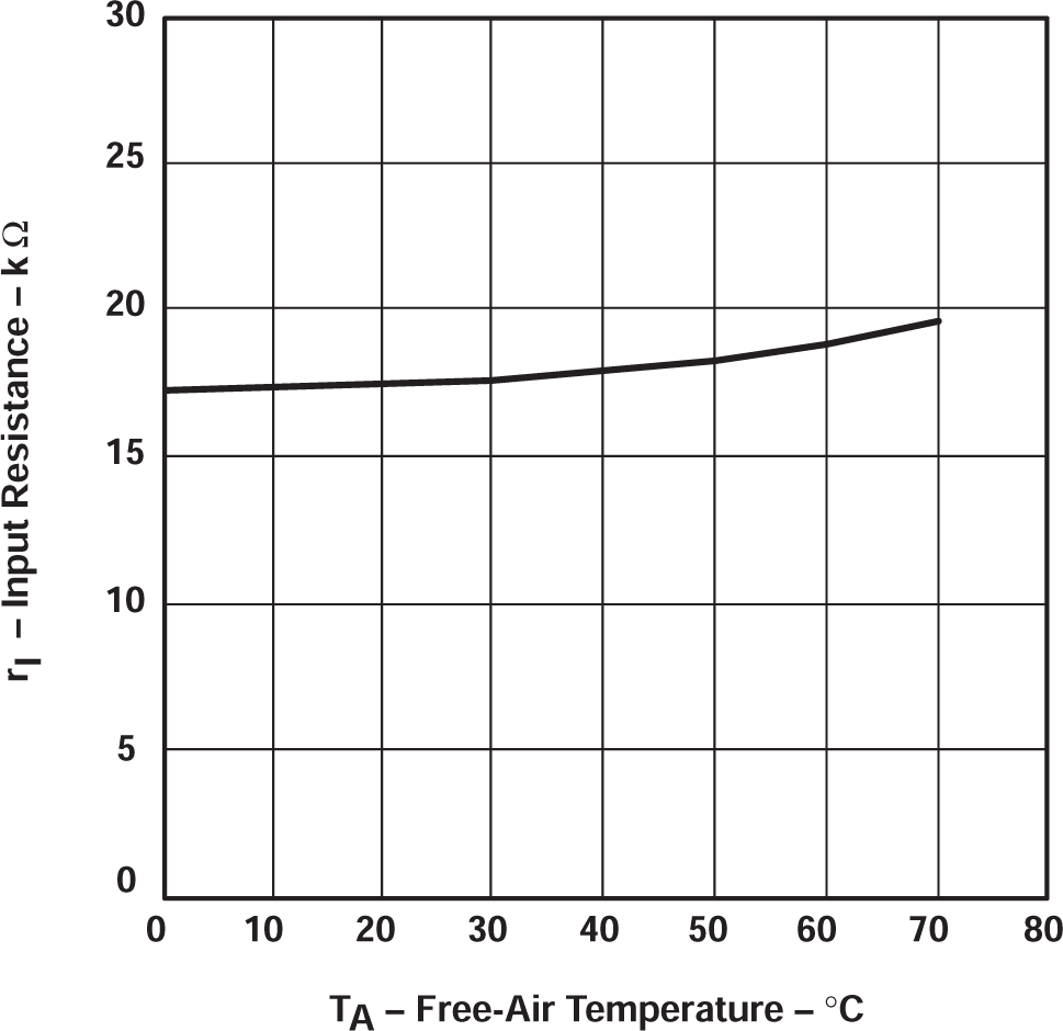 Figure 5-16 Input Resistance vs
Free-air Temperature
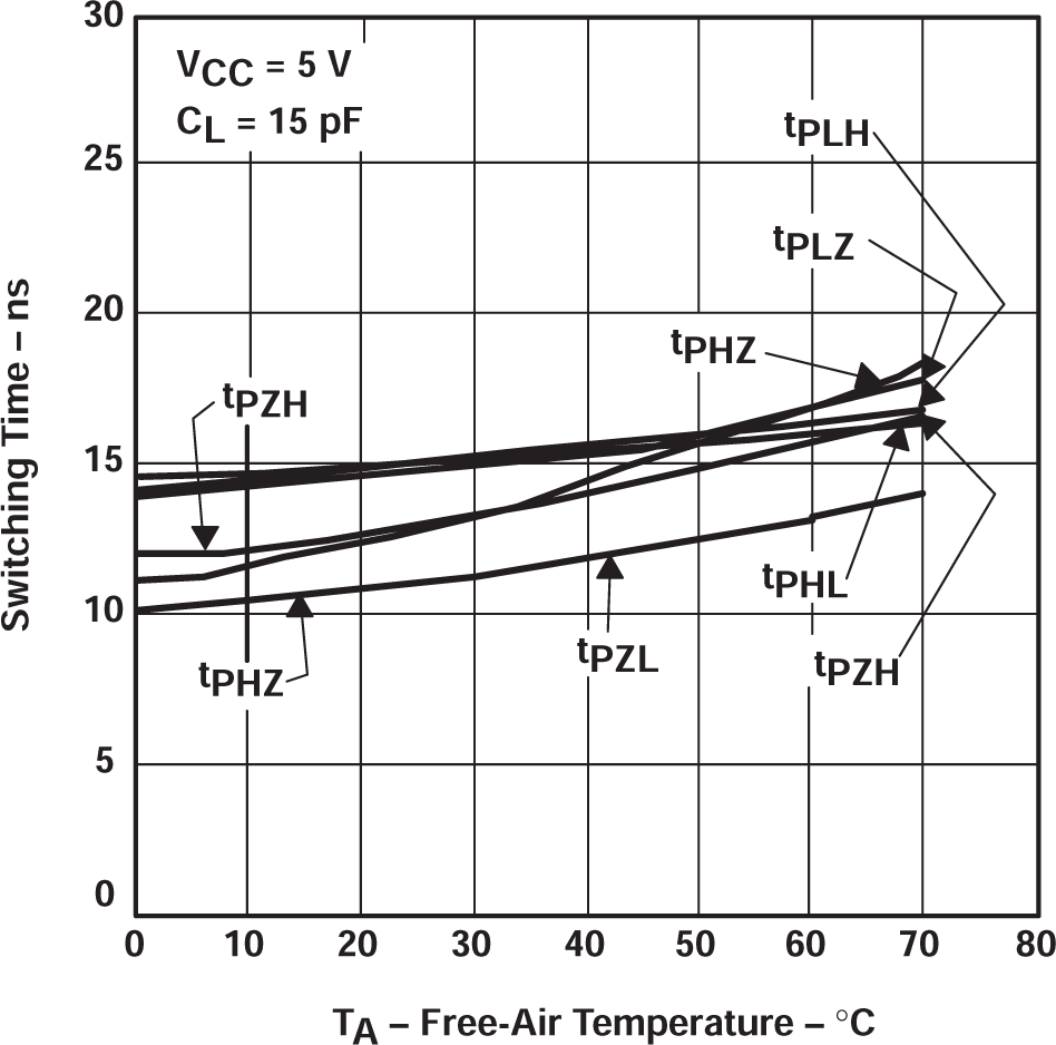 Figure 5-18 Switching Time vs Free-air
Temperature