SLLS045C January 1989 – October 2023 SN75ALS197
PRODUCTION DATA
- 1
- 1 Features
- 2 Applications
- 3 Description
- 4 Pin Configuration and Functions
- 5 Specifications
- 6 Parameter Measurement Information
- 7 Detailed Description
- 8 Device and Documentation Support
- 9 Revision History
- 10Mechanical, Packaging, and Orderable Information
Package Options
Refer to the PDF data sheet for device specific package drawings
Mechanical Data (Package|Pins)
- NS|16
- N|16
- D|16
Thermal pad, mechanical data (Package|Pins)
Orderable Information
3 Description
The SN75ALSI97 is a monolithic, quadruple line receiver with 3-state outputs designed using advanced, low-power, Schottky technology. This technology provides combined improvements in bar design, tooling production, and wafer fabrication. This, in turn, provides significantly lower power requirements and permits much higher data throughput than other designs. The device meets the specifications of ITU Recommendations V.10, V.11, X.26, and X.27. The 3-state outputs feature permits direct connection to a bus-organized system with a fail-safe design that makes sure the outputs is always high if the inputs are open.
The device is optimized for balanced, multipoint bus transmission at rates up to 20 megabits per second. The input features high-input impedance, input hysteresis for increased noise immunity, and an input sensitivity of ±300 mV over a common-mode input voltage range of −7 V to 7 V. The device also features active-high and active-low enable functions that are common to the four channels. The device is designed for optimum performance when used with the SN75ALS192 quadruple differential line driver.
The SN75ALS197 is characterized for operation from 0°C to 70°C.
| PART NUMBER | PACKAGE(1) | PACKAGE SIZE(2) |
|---|---|---|
| SN75ALS197 | SOIC (D, 16) | 9.9 mm × 6 mm |
| PDIP (N, 16) | 19.3 mm × 9.4 mm | |
| SO (NS, 16) | 10 mm × 7.8 mm |
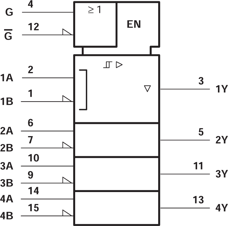
 Logic Symbol(1)
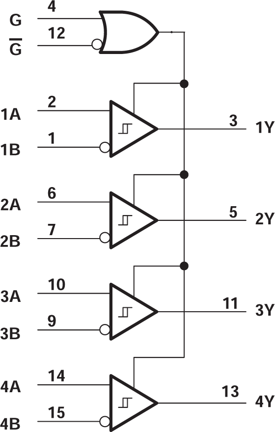
 Logic Diagram (Positive Logic)