SLLS725B June 2006 – August 2021 SN65C3222E , SN75C3222E
PRODUCTION DATA
- 1 Features
- 2 Applications
- 3 Description
- 4 Revision History
- 5 Pin Configuration and Functions
-
6 Specifications
- 6.1 Absolute Maximum Ratings
- 6.2 ESD Ratings
- 6.3 ESD Ratings - IEC Specifications
- 6.4 Recommended Operating Conditions
- 6.5 Thermal Information: SN65C3222E
- 6.6 Thermal Information: SN75C3222E
- 6.7 Electrical Characteristics
- 6.8 Electrical Characteristics: Driver
- 6.9 Switching Characteristics: Driver
- 6.10 Electrical Characteristics: Receiver
- 6.11 Switching Characteristics: Receiver
- 7 Parameter Measurement Information
- 8 Detailed Description
- 9 Application and Implementation
- 10Device and Documentation Support
- 11Mechanical, Packaging, and Orderable Information
Package Options
Mechanical Data (Package|Pins)
- PW|20
Thermal pad, mechanical data (Package|Pins)
Orderable Information
3 Description
The SN65C3222E and SN75C3222E consist of two line drivers, two line receivers, and a dual charge-pump circuit with ±15-kV ESD protection pin to pin (serial-port connection pins, including GND).
The devices meet the requirements of TIA/EIA-232-F and provide the electrical interface between an asynchronous communication controller and the serial-port connector. The charge pump and four small external capacitors allow operation from a single 3-V to 5.5-V supply. The devices operate at typical data signaling rates up to 1000 kbit/s and are improved drop-in replacements for industry-popular '3222 two-driver, two-receiver functions.
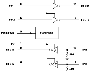
The SN65C3222E and SN75C3222E can be placed in the power-down mode by setting the power-down ( PWRDOWN) input low, which draws only 1 μA from the power supply. When the devices are powered down, the receivers remain active while the drivers are placed in the high-impedance state. Also, during power down, the onboard charge pump is disabled; V+ is lowered to VCC, and V– is raised toward GND. Receiver outputs also can be placed in the high-impedance state by setting enable ( EN) high.
| PART NUMBER | PACKAGE(1) | BODY SIZE (NOM) |
|---|---|---|
| SN65C3222E SN75C3222E | DB (SSOP) (20) | 10.2 mm x 5.30 mm |
| DW (SOIC) (20) | 15.4 mm x 7.50 mm | |
| PW (TSSOP) (20) | 7.80 mm v 4.40 mm |
