SLLSE12A November 2009 – July 2014 SN75DP119
PRODUCTION DATA.
- 1 Features
- 2 Applications
- 3 Description
- 4 Revision History
- 5 Description (continued)
- 6 Pin Configuration and Functions
- 7 Specifications
- 8 Parameter Measurement Information
- 9 Detailed Description
- 10Application and Implementation
- 11Power Supply Recommendations
- 12Layout
- 13Device and Documentation Support
- 14Mechanical, Packaging, and Orderable Information
Package Options
Mechanical Data (Package|Pins)
Thermal pad, mechanical data (Package|Pins)
Orderable Information
12 Layout
12.1 Layout Guidelines
- Data rates of 2.7Gbps require fast edge rate, which can cause EMI radiation if the pcb is not designed carefully.
- Decoupling with small current loops is recommended.
- It is recommended to place the de-coupling cap as close as possible to the device and on the same side of the pcb (see Figure 12).
- Choose the capacitor such that the resonant frequency of the capacitor does not align closely with 2.7GHz.
- Also provide several GND vias to the thermal pad to minimize the area of current loops.
12.2 Layout Example
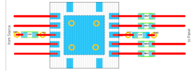 Figure 12. De-Coupling Layout Recommendation