SLLS163F July 1993 – April 2024 SN65LBC172 , SN75LBC172
PRODUCTION DATA
- 1
- 1 Features
- 2 Applications
- 3 Description
- 4 Pin Configuration and Functions
- 5 Specifications
- 6 Parameter Measurement Information
- 7 Detailed Description
- 8 Device and Documentation Support
- 9 Revision History
- 10Mechanical, Packaging, and Orderable Information
Package Options
Refer to the PDF data sheet for device specific package drawings
Mechanical Data (Package|Pins)
- N|16
- DW|20
Thermal pad, mechanical data (Package|Pins)
Orderable Information
3 Description
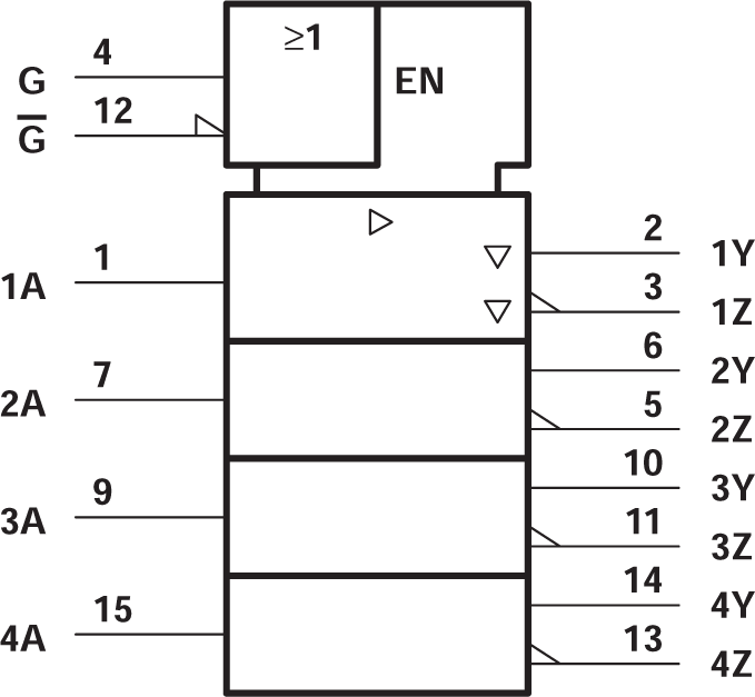
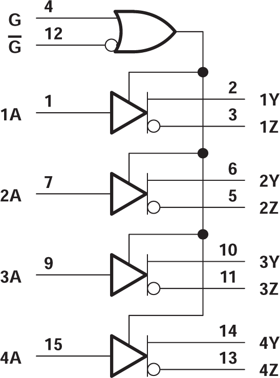
The SN65LBC172 and SN75LBC172 are monolithic quadruple differential line drivers with three-state outputs. Both devices are designed to meet the requirements of EIA Standard RS-485. These devices are optimized for balanced multipoint bus transmission at data rates up to and exceeding 10 million bits per second. Each driver features wide positive and negative common- mode output voltage ranges, current limiting, and thermal-shutdown circuitry which provides a party-line application in noisy environments. Both devices are designed using LinBiCMOS™, facilitating ultra-low power consumption and inherent robustness.
Both the SN65LBC172 and SN75LBC172 provide positive- and negative-current limiting and thermal shutdown for protection from line fault conditions on the transmission bus line. These devices offer optimum performance when used with the SN75LBC173 or SN75LBC175 quadruple line receivers. The SN65LBC172 and SN75LBC172 are available in the 16-pin DIP package (N) and the 20-pin wide-body small-outline inline-circuit (SOIC) package (DW).
The SN75LBC172 is characterized for operation over the commercial temperature range of 0°C to 70°C. The SN65LBC172 is characterized over the industrial temperature range of −40°C to 85°C.
| PART NUMBER | PACKAGE(1) | PACKAGE SIZE(2) |
|---|---|---|
| SN65LBC172 SN75LBC172 |
DW (SOIC, 20) | 10.3mm × 10.3mm |
| N (PDIP 16) | 19.3mm × 9.4mm |

