SLLS170F October 1993 – November 2023 SN65LBC173 , SN75LBC173
PRODUCTION DATA
- 1
- 1 Features
- 2 Applications
- 3 Description
- 4 Pin Configuration and Functions
- 5 Specifications
- 6 Parameter Measurement Information
- 7 Detailed Description
- 8 Device and Documentation Support
- 9 Revision History
- 10Mechanical, Packaging, and Orderable Information
Package Options
Mechanical Data (Package|Pins)
Thermal pad, mechanical data (Package|Pins)
Orderable Information
3 Description
The SN65LBC173 and SN75LBC173 are monolithic quadruple differential line receivers with 3-state outputs. Both are designed to meet the requirements of the ANSI standards EIA/TIA-422-B, EIA/TIA-423-B, RS-485, and ITU Recommendations V.10 and V.11. The devices are optimized for balanced multipoint bus transmission at data rates up to and exceeding 10 million bits per second. The four receivers share two ORed enable inputs, one active when high, the other active when low.
Each receiver features high input impedance, input hysteresis for increased noise immunity, and input sensitivity of ±200 mV over a common-mode input voltage range of 12 V to −7 V. Fail-safe design ensures that if the inputs are open circuited, the output is always high. Both devices are designed using the Texas Instruments proprietary LinBiCMOS™ technology that provides low power consumption, high switching speeds, and robustness.
These devices offer optimum performance when used with the SN75LBC172 or SN75LBC174 quadruple line drivers. The SN65LBC173 and SN75LBC173 are available in the 16-pin DIP (N) and SOIC (D) packages.
The SN65LBC173 is characterized over the industrial temperature range of −40°C to 85°C. The SN75LBC173 is characterized for operation over the commercial temperature range of 0°C to 70°C.
| PART NUMBER | PACKAGE(1) | PACKAGE SIZE(2) |
|---|---|---|
| SN65LBC173 SN75LBC173 |
D (SOIC, 16) | 9.9 mm × 6 mm |
| N (PDIP, 16) | 19.3 mm × 9.4 mm |
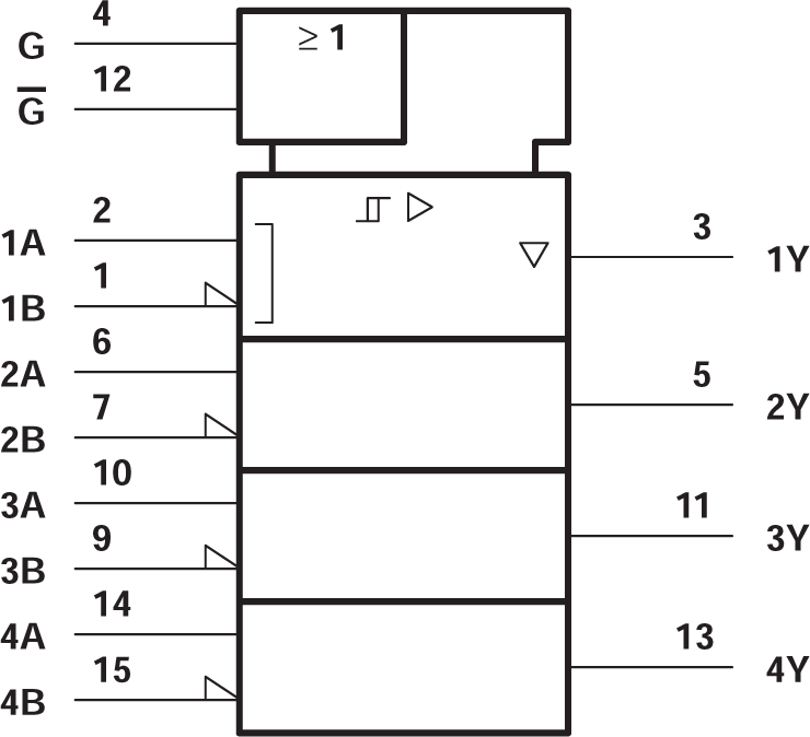
 Logic Symbol(1)
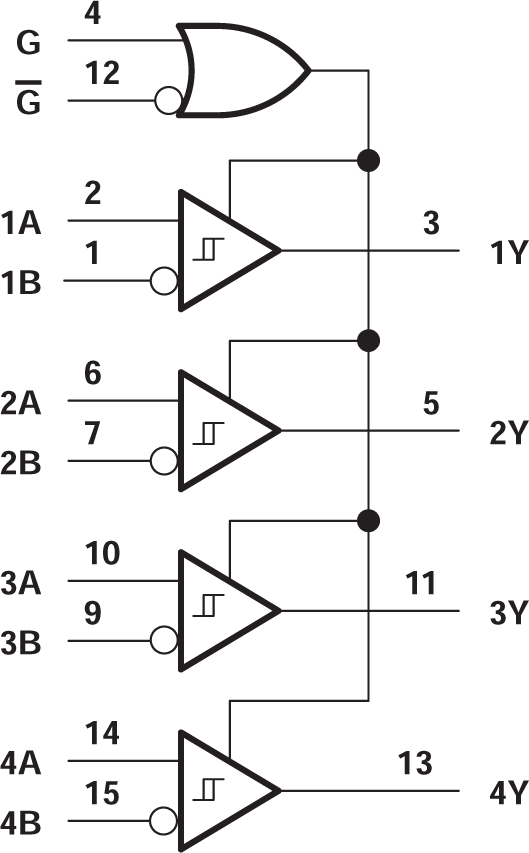
 Logic Diagram (Positive Logic)