SLLS173G January 1994 – October 2022 SN65LBC179 , SN75LBC179
PRODUCTION DATA
- 1Features
- 2Description
- 3Revision History
- 4Pin Configuration and Functions
-
5Specifications
- 5.1 Absolute Maximum Ratings
- 5.2 Recommended Operating Conditions
- 5.3 Thermal Information
- 5.4 Dissipation Rating Table
- 5.5 Electrical Characteristics - Driver
- 5.6 Switching Characteristics - Driver
- 5.7 Electrical Characteristics - Receiver
- 5.8 Switching Characteristics - Receiver
- 5.9 Typical Characteristics
- 6Parameter Measurement Information
- 7Detailed Description
- 8Device and Documentation Support
- 9Mechanical, Packaging, and Orderable Information
Package Options
Mechanical Data (Package|Pins)
- P|8
Thermal pad, mechanical data (Package|Pins)
Orderable Information
2 Description
The SN65LBC179, SN65LBC179Q, and SN75LBC179 differential driver and receiver pairs are monolithic integrated circuits designed for bidirectional data communication over long cables that take on the characteristics of transmission lines. The devices are balanced, or differential, voltage mode devices that meet or exceed the requirements of industry standards ANSIRS-485 and ISO 8482:1987(E). Both devices are designed using TI’s proprietary LinBiCMOS™ with the low power consumption of CMOS and the precision and robustness of bipolar transistors in the same circuit.
The SN65LBC179, SN65LBC179Q, and SN75LBC179 combine a differential line driver and differential line receiver and operate from a single 5-V supply. The driver differential outputs and the receiver differential inputs are connected to separate terminals for full-duplex operation and are designed to present minimum loading to the bus when powered off (VCC = 0). These parts feature a wide common-mode voltage range making them suitable for point-to-point or multipoint data bus applications. The devices also provide positive and negative-current limiting and thermal shutdown for protection from line fault conditions. The line driver shuts down at a junction temperature of approximately 172°C.
The SN65LBC179, SN65LBC179Q, and SN75LBC179 are available in the 8-pin dual-in-line and small-outline packages. The SN75LBC179 is characterized for operation over the commercial temperature range of 0°C to 70°C. The SN65LBC179 is characterized over the industrial temperature range of −40°C to 85°C. The SN65LBC179Q is characterized over the extended industrial or automotive temperature range of −40°C to 125°C.
| PART NUMBER | PACKAGE(1) | BODY SIZE (NOM) |
|---|---|---|
| SN75179B | D (SOIC) | 4.9 mm x 3.91 mm |
| P (PDIP) | 9.81 mm x 6.35 mm |

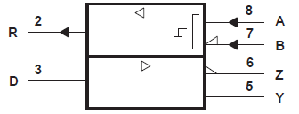
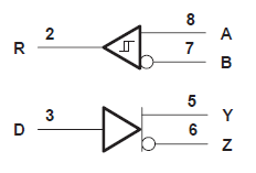
 Logic Diagram (Positive Logic)