SLLS377E May 2000 – January 2023 SN65LBC179A , SN75LBC179A
PRODUCTION DATA
- 1Features
- 2Description
- 3Revision History
- 4Pin Configuration and Functions
- 5Specifications
- 6Parameter Measurement Information
- 7Detailed Description
- 8Device and Documentation Support
- 9Mechanical, Packaging, and Orderable Information
Package Options
Mechanical Data (Package|Pins)
Thermal pad, mechanical data (Package|Pins)
Orderable Information
5.9 Typical Characteristics
 Figure 5-1 Typical Waveform of Non-Return-To-Zero (NRZ), Pseudorandom Binary Sequence (PRBS) Data at 100 Mbps Through 15m, of CAT 5 Unshielded Twisted Pair (UTP) Cable
TIA/EIA-485-A defines a maximum signaling rate as that in which the transition time of the voltage transition of a logic-state change remains less than or equal to 30% of the bit length. Transition times of greater length perform quite well even though they do not meet the standard by definition.
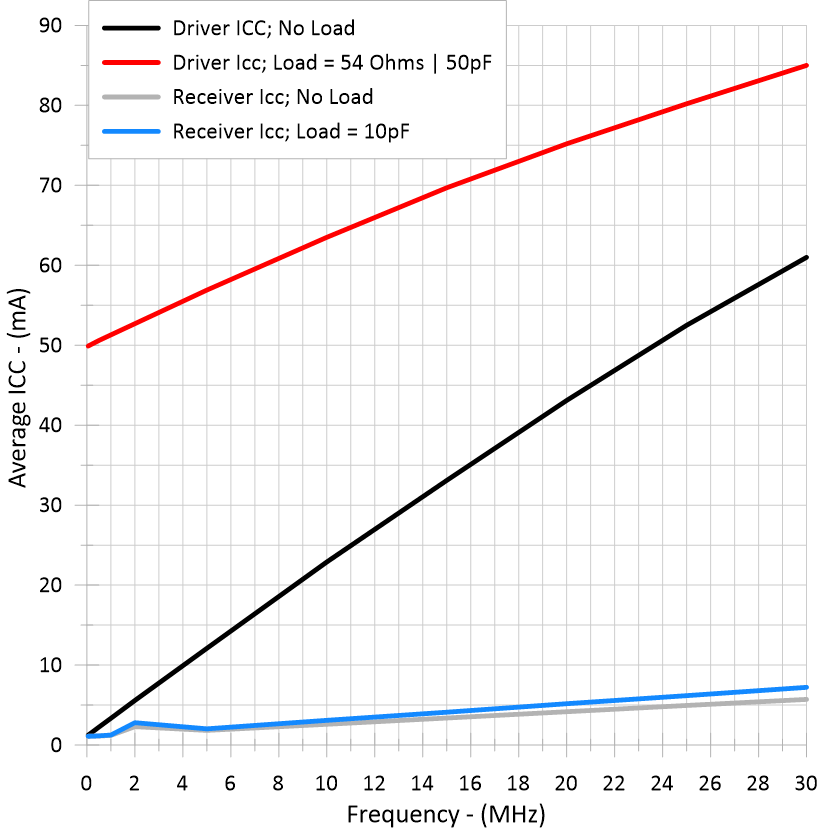 Figure 5-2 Average Supply Current vs
Frequency
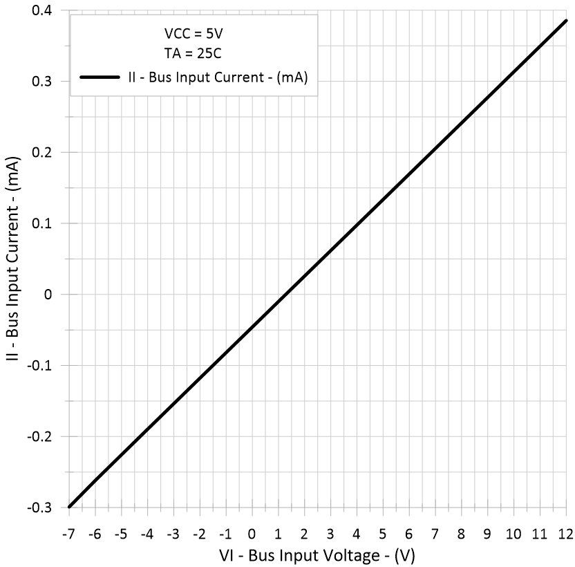 Figure 5-4 Input Current vs Input
Voltage
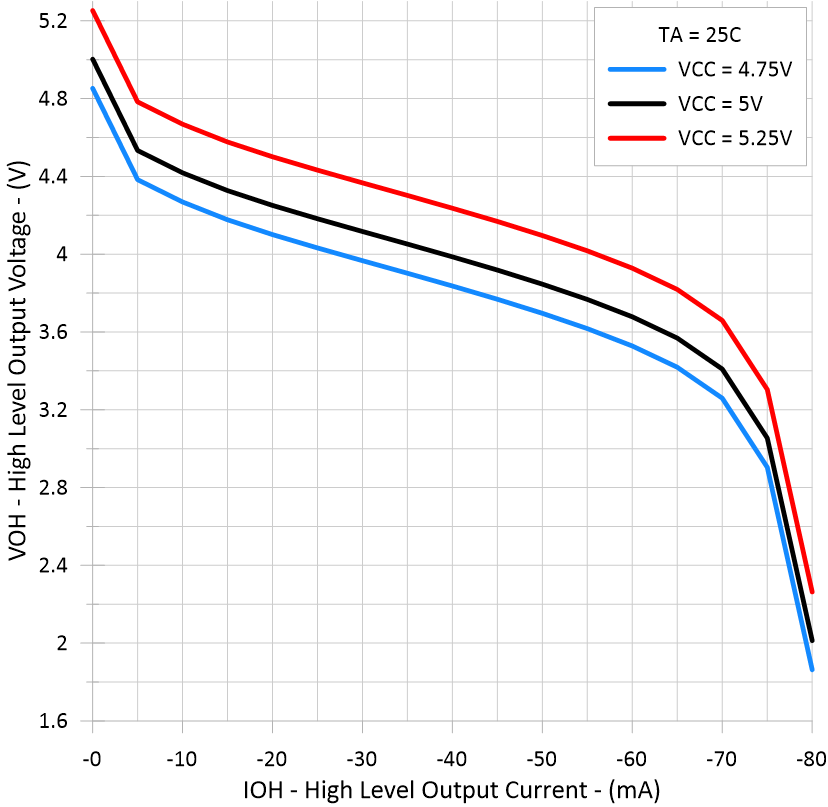 Figure 5-6 Driver High-Level Output
Voltage vs HIGH-Level Output Current
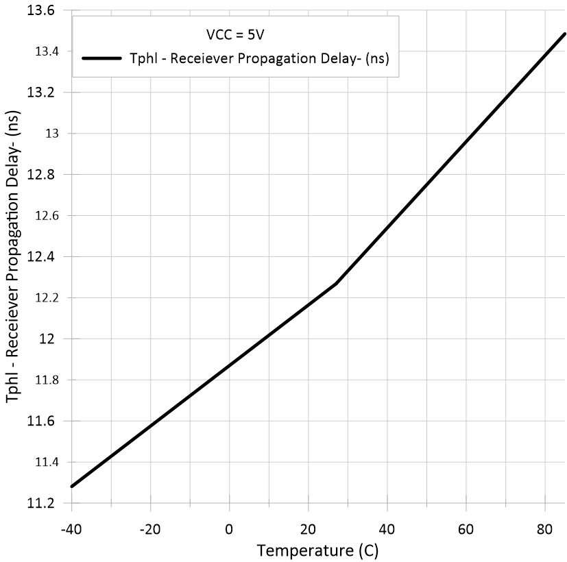 Figure 5-8 Receiver Propagation Time
vs Case Temperature
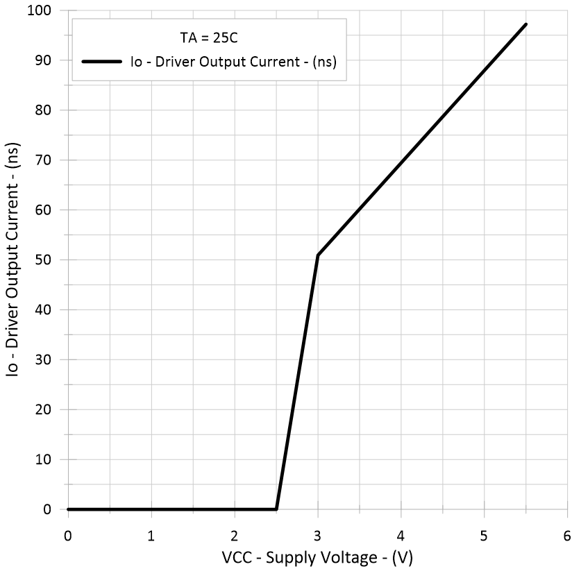 Figure 5-10 Driver Output Current vs
Supply Voltage
 Figure 5-3 Logic Input Current vs
Input Voltage
 Figure 5-5 Low-Level Output Voltage
vs Low-Level Output Current
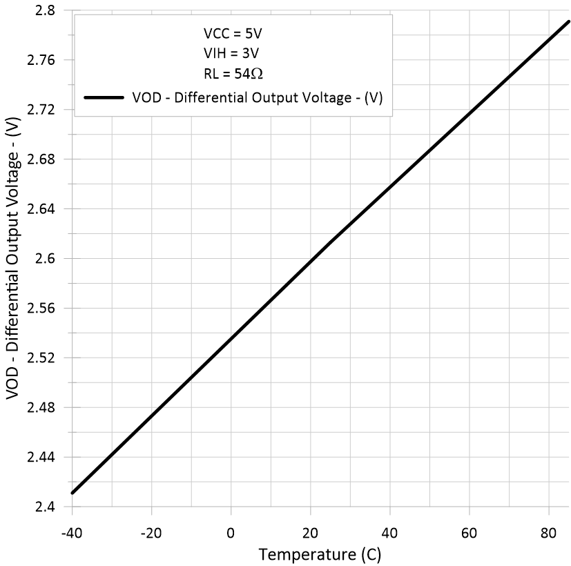 Figure 5-7 Driver Differential Output
Voltage vs Average Case Temperature
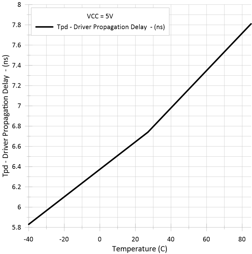 Figure 5-9 Driver Propagation Delay
Time vs Case Temperature