SLLS174I February 1994 – October 2022 SN55LBC180 , SN65LBC180 , SN75LBC180
PRODUCTION DATA
- 1 Features
- 2 Description
- 3 Description (Continued)
- 4 Revision History
- 5 Pin Configuration and Functions
- 6 Specifications
- 7 Parameter Measurement Information
- 8 Detailed Description
- 9 Application and Implementation
- 10Device and Documentation Support
- 11Mechanical, Packaging, and Orderable Information
Package Options
Refer to the PDF data sheet for device specific package drawings
Mechanical Data (Package|Pins)
- N|14
Thermal pad, mechanical data (Package|Pins)
Orderable Information
7 Parameter Measurement Information
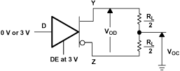
 Figure 7-1 Differential and Common-Mode Output Voltages
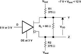
 Figure 7-2 Driver VOD Test Circuit
 Figure 7-3 Driver Test Circuit and Differential Output Delay and Transition Time Voltage Waveforms
 Figure 7-4 Driver Test Circuit and Enable and Disable Time Waveforms
 Figure 7-5 Driver Test Circuit and Enable and Disable Time Voltage Waveforms
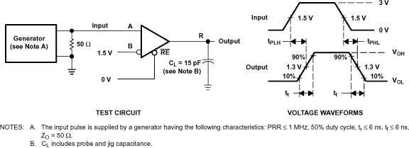
 Figure 7-6 Receiver Test Circuit and Propagation Delay Time Voltage Waveforms
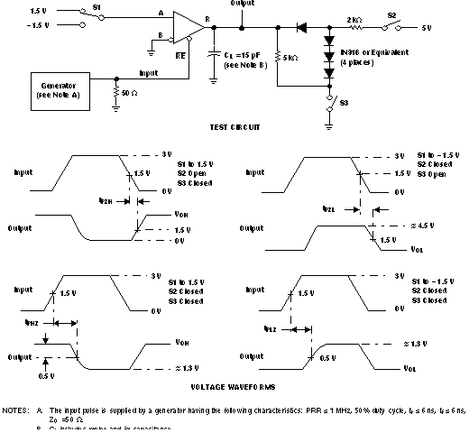
 Figure 7-7 Receiver Output Enable and Disable Times