SLLS378E May 2000 – January 2023 SN65LBC180A , SN75LBC180A
PRODUCTION DATA
- 1Features
- 2Description
- 3Revision History
- 4Pin Configuration and Functions
- 5Reference
- 6Detailed Description
- 7Application Information
- 8Device and Documentation Support
- 9Mechanical, Packaging, and Orderable Information
Package Options
Refer to the PDF data sheet for device specific package drawings
Mechanical Data (Package|Pins)
- N|14
Thermal pad, mechanical data (Package|Pins)
Orderable Information
2 Description
The SN65LBC180A and SN75LBC180A differential driver and receiver pairs are monolithic integrated circuits designed for bidirectional data communication over long cables that take on the characteristics of transmission lines. They are balanced, or differential, voltage mode devices that are compatible with ANSI standard TIA/EIA-485-A and ISO 8482:1987(E). The A version offers improved switching performance over its predecessors without sacrificing significantly more power.
These devices combine a differential line driver and differential input line receiver and operate from a single 5-V power supply. The driver differential outputs and the receiver differential inputs are connected to separate terminals for full-duplex operation and are designed to present minimum loading to the bus when powered off (VCC = 0). These parts feature wide positive and negative common-mode voltage ranges, making them suitable for point-to-point or multipoint data bus applications. The devices also provide positive and negative current limiting for protection from line fault conditions. The SN65LBC180A is characterized for operation from –40°C to 85°C, and the SN75LBC180A is characterized for operation from 0°C to 70°C.
| PART NUMBER | PACKAGE(1) | BODY SIZE (NOM) |
|---|---|---|
| SN65LBC180ASN75LBC180A | D (SOIC) | 4.9 mm x 3.91 mm |
| N (PDIP) | 9.81 mm x 6.35 mm |
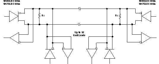
 Typical Application