SLLS236J October 1996 – July 2024 SN65LBC184 , SN75LBC184
PRODUCTION DATA
- 1
- 1 Features
- 2 Applications
- 3 Description
- 4 Pin Configuration and Functions
-
5 Specifications
- 5.1 Absolute Maximum Ratings
- 5.2 ESD Ratings
- 5.3 Recommended Operating Conditions
- 5.4 Thermal Information
- 5.5 Electrical Characteristics: Driver
- 5.6 Electrical Characteristics: Receiver
- 5.7 Driver Switching Characteristics
- 5.8 Receiver Switching Characteristics
- 5.9 Dissipation Ratings
- 5.10 Typical Characteristics
- 6 Parameter Measurement Information
- 7 Detailed Description
- 8 Application and Implementation
- 9 Device and Documentation Support
- 10Revision History
- 11Mechanical, Packaging, and Orderable Information
Package Options
Mechanical Data (Package|Pins)
Thermal pad, mechanical data (Package|Pins)
Orderable Information
8.2.3 Application Curve
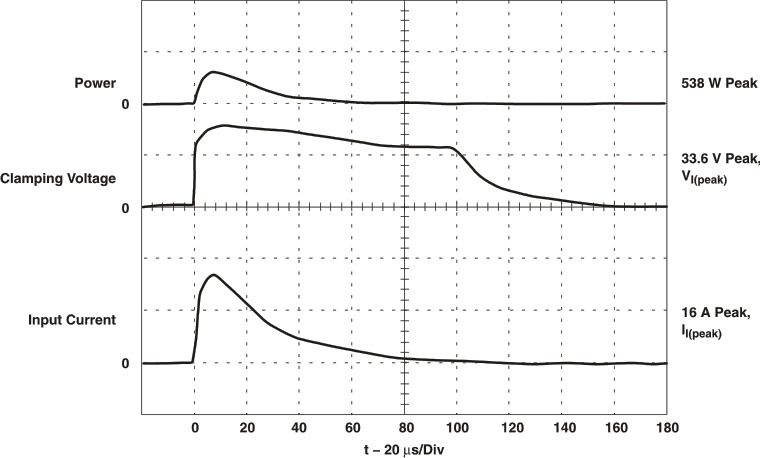
An example waveform as seen by the SN65LBC184 is shown in Figure 8-6. The bottom trace is current, the middle trace shows the clamping voltage of the device and the top trace is power as calculated from the voltage and current waveforms. This example shows a peak clamping voltage of 33.6V and peak current of 16A, thus yielding an absorbed peak power of 538W.
 Figure 8-6 Typical Surge Waveform Measured at Pins 5 and 7