SLLS362G SEPTEMBER   1999  – January 2016 SN65LVDS387 , SN65LVDS389 , SN65LVDS391 , SN75LVDS387 , SN75LVDS389 , SN75LVDS391

PRODUCTION DATA.  

  1. Features
  2. Applications
  3. Description
  4. Revision History
  5. Description (Continued)
  6. Device Options
  7. Pin Configuration and Functions
  8. Specifications
    1. 8.1 Absolute Maximum Ratings
    2. 8.2 ESD Ratings
    3. 8.3 Recommended Operating Conditions
    4. 8.4 Thermal Information
    5. 8.5 Electrical Characteristics
    6. 8.6 Switching Characteristics
    7. 8.7 Typical Characteristics
  9. Parameter Measurement Information
  10. 10Detailed Description
    1. 10.1 Overview
    2. 10.2 Functional Block Diagram
    3. 10.3 Feature Description
      1. 10.3.1 Driver Output Voltage and Power-On Reset
      2. 10.3.2 5-V Input Tolerance
      3. 10.3.3 NC Pins
      4. 10.3.4 Unused Enable Pins
      5. 10.3.5 Driver Equivalent Schematics
    4. 10.4 Device Functional Modes
  11. 11Application and Implementation
    1. 11.1 Application Information
      1. 11.1.1 Signaling Rate vs Distance
    2. 11.2 Typical Application
      1. 11.2.1 Point-to-Point Communications
        1. 11.2.1.1 Design Requirements
        2. 11.2.1.2 Detailed Design Procedure
          1. 11.2.1.2.1 Driver Supply Voltage
          2. 11.2.1.2.2 Driver Bypass Capacitance
          3. 11.2.1.2.3 Driver Output Voltage
          4. 11.2.1.2.4 Interconnecting Media
          5. 11.2.1.2.5 PCB Transmission Lines
          6. 11.2.1.2.6 Termination Resistor
          7. 11.2.1.2.7 Driver NC Pins
        3. 11.2.1.3 Application Curve
      2. 11.2.2 Multidrop Communications
        1. 11.2.2.1 Design Requirements
        2. 11.2.2.2 Detailed Design Procedure
          1. 11.2.2.2.1 Interconnecting Media
        3. 11.2.2.3 Application Curve
  12. 12Power Supply Recommendations
  13. 13Layout
    1. 13.1 Layout Guidelines
      1. 13.1.1 Microstrip vs Stripline Topologies
      2. 13.1.2 Dielectric Type and Board Construction
      3. 13.1.3 Recommended Stack Layout
      4. 13.1.4 Separation Between Traces
      5. 13.1.5 Crosstalk and Ground Bounce Minimization
    2. 13.2 Layout Example
  14. 14Device and Documentation Support
    1. 14.1 Device Support
      1. 14.1.1 Third-Party Products Disclaimer
      2. 14.1.2 Other LVDS Products
    2. 14.2 Documentation Support
      1. 14.2.1 Related Information
    3. 14.3 Related Links
    4. 14.4 Trademarks
    5. 14.5 Electrostatic Discharge Caution
    6. 14.6 Glossary
  15. 15Mechanical, Packaging, and Orderable Information

Package Options

Refer to the PDF data sheet for device specific package drawings

Mechanical Data (Package|Pins)
  • PW|16
  • D|16
Thermal pad, mechanical data (Package|Pins)
Orderable Information

7 Pin Configuration and Functions
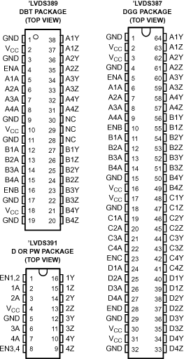
SN65LVDS387 SN75LVDS387 SN65LVDS389 SN75LVDS389 SN65LVDS391 SN75LVDS391 po3_lls362.gif

Pin Functions: SNx5LVDS391

PIN I/O DESCRIPTION
NAME NUMBER
VCC 4 Supply voltage
GND 5 Ground
1A 2 I LVTTL input signal
1Y 16 O Differential (LVDS) non-inverting output
1Z 15 O Differential (LVDS) inverting output
2A 3 I LVTTL input signal
2Y 14 O Differential (LVDS) non-inverting output
2Z 13 O Differential (LVDS) inverting output
3A 6 I LVTTL input signal
3Y 12 O Differential (LVDS) non-inverting output
3Z 11 O Differential (LVDS) inverting output
4A 7 I LVTTL input signal
4Y 10 O Differential (LVDS) non-inverting output
4Z 9 O Differential (LVDS) inverting output
EN1,2 1 I Enable for channels 1 and 2
EN3,4 8 I Enable for channels 3 and 4

Pin Functions: SNx5LVDS389

PIN I/O DESCRIPTION
NAME NUMBER
VCC 2, 10, 18 Supply voltage
GND 1, 3, 9, 11, 17, 19 Ground
A1A 5 I LVTTL input signal
A1Y 38 O Differential (LVDS) non-inverting output
A1Z 37 O Differential (LVDS) inverting output
A2A 6 I LVTTL input signal
A2Y 36 O Differential (LVDS) non-inverting output
A2Z 35 O Differential (LVDS) inverting output
A3A 7 I LVTTL input signal
A3Y 34 O Differential (LVDS) non-inverting output
A3Z 33 O Differential (LVDS) inverting output
A4A 8 I LVTTL input signal
A4Y 32 O Differential (LVDS) non-inverting output
A4Z 31 O Differential (LVDS) inverting output
B1A 12 I LVTTL input signal
B1Y 27 O Differential (LVDS) non-inverting output
B1Z 26 O Differential (LVDS) inverting output
B2A 13 I LVTTL input signal
B2Y 25 O Differential (LVDS) non-inverting output
B2Z 24 O Differential (LVDS) inverting output
B3A 14 I LVTTL input signal
B3Y 23 O Differential (LVDS) non-inverting output
B3Z 22 O Differential (LVDS) inverting output
B4A 15 I LVTTL input signal
B4Y 21 O Differential (LVDS) non-inverting output
B4B 20 O Differential (LVDS) inverting output
ENA 4 I Enable for channel A
ENB 16 I Enable for channel B
NC 28, 29, 30 No connection

Pin Functions: SNx5LVDS387

PIN I/O DESCRIPTION
NAME NUMBER
VCC 2, 3, 16, 17, 30, 31 Supply voltage
GND 1, 4, 15, 18, 29, 32 Ground
A1A 6 I LVTTL input signal
A1Y 64 O Differential (LVDS) non-inverting output
A1Z 73 O Differential (LVDS) inverting output
A2A 7 I LVTTL input signal
A2Y 62 O Differential (LVDS) non-inverting output
A2Z 61 O Differential (LVDS) inverting output
A3A 8 I LVTTL input signal
A3Y 60 O Differential (LVDS) non-inverting output
A3Z 59 O Differential (LVDS) inverting output
A4A 9 I LVTTL input signal
A4Y 58 O Differential (LVDS) non-inverting output
A4Z 57 O Differential (LVDS) inverting output
B1A 11 I LVTTL input signal
B1Y 56 O Differential (LVDS) non-inverting output
B1Z 55 O Differential (LVDS) inverting output
B2A 12 I LVTTL input signal
B2Y 54 O Differential (LVDS) non-inverting output
B2Z 53 O Differential (LVDS) inverting output
B3A 13 I LVTTL input signal
B3Y 52 O Differential (LVDS) non-inverting output
B3Z 51 O Differential (LVDS) inverting output
B4A 14 I LVTTL input signal
B4Y 50 O Differential (LVDS) non-inverting output
B4B 49 O Differential (LVDS) inverting output
C1A 19 I LVTTL input signal
C1Y 48 O Differential (LVDS) non-inverting output
C1Z 47 O Differential (LVDS) inverting output
C2A 20 I LVTTL input signal
C2Y 46 O Differential (LVDS) non-inverting output
C2Z 45 O Differential (LVDS) inverting output
C3A 21 I LVTTL input signal
C3Y 44 O Differential (LVDS) non-inverting output
C3Z 43 O Differential (LVDS) inverting output
C4A 22 I LVTTL input signal
C4Y 42 O Differential (LVDS) non-inverting output
C4Z 41 O Differential (LVDS) inverting output
D1A 24 I LVTTL input signal
D1Y 40 O Differential (LVDS) non-inverting output
D1Z 39 O Differential (LVDS) inverting output
D2A 25 I LVTTL input signal
D2Y 38 O Differential (LVDS) non-inverting output
D2Z 37 O Differential (LVDS) inverting output
D3A 26 I LVTTL input signal
D3Y 36 O Differential (LVDS) non-inverting output
D3Z 35 O Differential (LVDS) inverting output
D4A 27 I LVTTL input signal
D4Y 34 O Differential (LVDS) non-inverting output
B4B 33 O Differential (LVDS) inverting output
ENA 5 I Enable for channel A
ENB 10 I Enable for channel B
ENC 23 I Enable for channel C
END 26 I Enable for channel D