SLLS259J November 1996 – October 2016 SN75LVDS82
PRODUCTION DATA.
- 1 Features
- 2 Applications
- 3 Description
- 4 Revision History
- 5 Description (continued)
- 6 Pin Configuration and Functions
- 7 Specifications
- 8 Parameter Measurement Information
- 9 Detailed Description
- 10Application and Implementation
- 11Power Supply Recommendations
- 12Layout
- 13Device and Documentation Support
- 14Mechanical, Packaging, and Orderable Information
Package Options
Mechanical Data (Package|Pins)
- DGG|56
Thermal pad, mechanical data (Package|Pins)
Orderable Information
10 Application and Implementation
NOTE
Information in the following applications sections is not part of the TI component specification, and TI does not warrant its accuracy or completeness. TI’s customers are responsible for determining suitability of components for their purposes. Customers should validate and test their design implementation to confirm system functionality.
10.1 Application Information
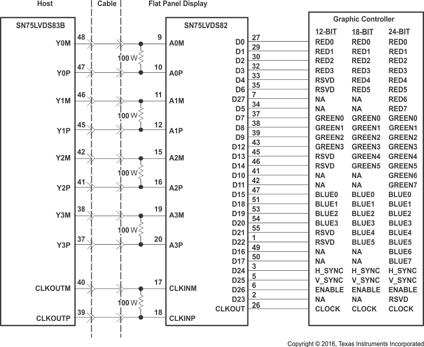
This section describes provides information on how each signal should be connected from the graphic source through the SN75LVDS83B and the SN75LVDS82 to the LCD panel input.
10.2 Typical Applications
10.2.1 Signal Connectivity

10.2.1.1 Design Requirements
For this design example, use the parameters shown in Table 2.
Table 2. Design Parameters
| DESIGN PARAMETERS | VALUE |
|---|---|
| VDD Main Power Supply | 3.3 V |
| Input LVDS Clock Frequency | 31 - 68 MHz |
| RL Differential Input Termination Resistance | 100 Ω |
| LVDS Input Lanes | 4 |
| Color depth | 24 Bit |
10.2.1.2 Detailed Design Procedure
10.2.1.2.1 Power Up Sequence
The user experience can be impacted by the way a system powers up and powers down an LCD screen. The following sequence is recommended.
Power up sequence (SN75LVDS82 /SHTDN input initially low):
- Ramp up LCD power (maybe 0.5 ms to 10 ms) but keep backlight turned off.
- Wait for additional 0-200 ms to ensure display noise will not occur.
- Enable video source output; start sending black video data.
- Toggle SN75LVDS82 shutdown to SHTDN = VIH.
- Send > 1 ms of black video data; this allows the SN75LVDS82 to be phase locked, and the display to show black data first.
- Start sending true image data.
- Enable backlight.
Power Down sequence (SN75LVDS82 SHTDN input initially high):
- Disable LCD backlight; wait for the minimum time specified in the LCD data sheet for the backlight to go low
- Video source output data switch from active video data to black image data (all visible pixel turn black); drive this for > 2 frame times.
- Set SN75LVDS82 input SHTDN = GND; wait for 250 ns.
- Disable the video output of the video source.
- Remove power from the LCD panel for lowest system power.
10.2.1.3 Application Curves
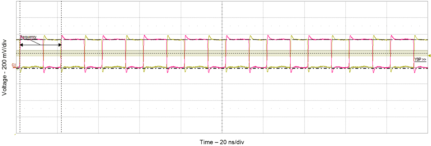
 Figure 17. LVDS Clock
 Figure 18. Output Clock