SLLSFY8 October 2024 SN75LVPE3101
PRODUCTION DATA
- 1
- 1 Features
- 2 Applications
- 3 Description
- 4 Pin Configuration and Functions
- 5 Specifications
- 6 Detailed Description
- 7 Application and Implementation
- 8 Device and Documentation Support
- 9 Revision History
- 10Mechanical, Packaging, and Orderable Information
Package Options
Mechanical Data (Package|Pins)
- RGE|24
Thermal pad, mechanical data (Package|Pins)
- RGE|24
Orderable Information
7.2.2 Detailed Design Procedure
In this example, the SN75LVPE3101 has a DC gain fixed at 0dB and a linearity range fixed at 1200mV. The SN75LVPE3101 performs far-end receiver termination detection and enables both upstream and downstream paths when far-end termination is detected on both TX1 and TX2.
The AC-coupling capacitor range defined for a SATA device is a lot smaller than the AC-coupling capacitor range defined for SATA Express and PCI Express (PCIe) as indicated by Figure 7-2. While the SN75LVPE3101 can usually detect the receiver termination of the PCIe and SATA Express device, a SATA 12nF (maximum) AC-coupling capacitor prevents the SN75LVPE3101 from detecting the SATA device receiver termination. To correct this problem, a ferrite bead along with 49.9Ω resistor must be placed between CTX2 and the miniCard/mSATA socket. These components can be isolated from the high-speed channel when PCIe or SATA Express is active by using an NFET as shown in Figure 7-4. TI recommends to enable the NFET whenever a SATA device is present. The ferrite bead chosen must present at least 600Ω impedance at 100MHz so as to not impact high-speed signaling. TI recommends to use Murata BLM03AG601SN1 or BLM03HD601SN1D or a ferrite bead with similar characteristics from a different vendor. For applications which only require support for PCIe and SATA Express and do not need to support SATA, the ferrite beads and 49.9Ω resistors are not needed.
 Figure 7-2 AC-Coupling Capacitor Implementation for SATA, SATA Express, and PCIe Devices
The SN75LVPE3101 power is at P(ACTIVE_1200mV) when both the upstream and downstream paths are enabled. To save system power in system S3/S4/S5 states, TI recommends to control the SN75LVPE3101 EN pin. Any time the system enters a low power state (S3, S4, or S5), TI recommends to deassert the EN pin. While the EN pin is deasserted, the SN75LVPE3101 consumes P(SHUTDOWN). Assertion of this pin is necessary any time the system exits a lower power state.
The SN75LVPE3101 compensates for channel loss in both the upstream (C to D) and downstream direction (A to B). Configure the CH1_EQ[2:1] and CH2_EQ[2:1] pins to the equalization setting that matches as close possible to the channel insertion loss. In this particular example, CH2_EQ[2:1] is for path A to B which is the channel between the PCIe/SATA/SATA Express host and the SN75LVPE3101, and CH1_EQ[2:1] is for path C to D which is the channel between the SN75LVPE3101 and the miniCard/mSATA socket.
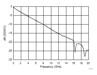
In this particular example, the channel A-B has a trace length of 8 inches with a 4mil trace width. This particular channel has about 0.83dB per inch of insertion loss at 5GHz. This equates to approximately 6.7dB of loss for the entire 8 inches of trace as depicted in Figure 7-3. An additional 1.5dB of loss is added due to package of the PCIe/SATA/SATA Express host, SN75LVPE3101, and the AC-coupling capacitor. This brings the entire channel loss at 5GHz to 6.7dB + 1.5dB = 8.2dB. The channel A-B for this example is connected to SN75LVPE3101 RX2P/N input and therefore CH2_EQ[2:1] pins are used for adjusting SN75LVPE3101 RX2P/N equalization settings. Set the CH2_EQ[2:1] pins such that SN75LVPE3101 equalization is between 5dB and 8dB. A value closer to 5dB may be best if the host has transmitter de-emphasis.

| Freq = 5GHz | dB(SDD21) = –6.666 |
Use a similar method for the upstream path (C to D). In this particular example, C to D has a trace length of 2 inches with a 4mil trace width. This equates to approximately 1.5dB at 5GHz. The SATA/SATA Express/PCIe device has a channel loss that can be added to the C to D channel loss. For this example, assume a value of 5dB is acceptable to compensate for C to D channel loss as well as loss associated with the SATA/SATA Express/PCIe device. Set the CH1_EQ[2:1] pins such that the SN75LVPE3101 equalization is 5dB.
 Figure 7-4 Example SATA/PCIe/SATA Express Schematic