SNLS666 January 2020 SN75LVPE4410
PRODUCTION DATA.
- 1 Features
- 2 Applications
- 3 Description
- 4 Revision History
- 5 Pin Configuration and Functions
- 6 Specifications
- 7 Detailed Description
- 8 Application and Implementation
- 9 Power Supply Recommendations
- 10Layout
- 11Device and Documentation Support
- 12Mechanical, Packaging, and Orderable Information
Package Options
Mechanical Data (Package|Pins)
- RNQ|40
Thermal pad, mechanical data (Package|Pins)
Orderable Information
6.8 Typical Characteristics
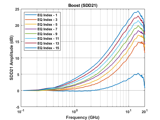 Figure 1. Typical EQ Boost vs Frequency for 8 (Out of Available 16) EQ Indices
 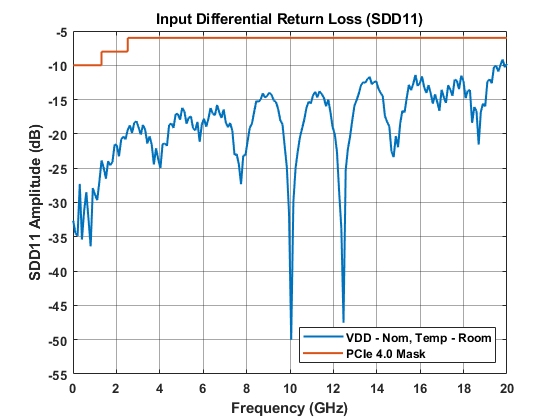 Figure 3. Typical Input (RX) Differential Return Loss vs Frequency in TI Evaluation Board with ~2 dB input and ~2 dB output loss
 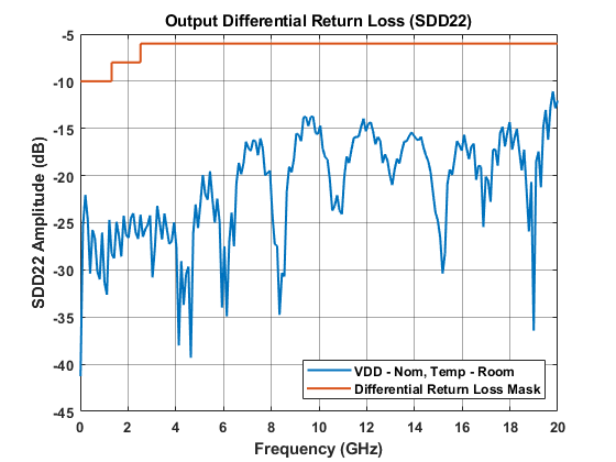 Figure 5. Typical Output (TX) Differential Return Loss vs Frequency in TI Evaluation Board with ~2 dB Input and ~2 dB Output Loss
 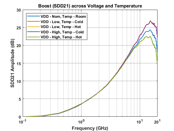 Figure 2. EQ Boost vs Frequency with EQ Index 15 (Maximum Setting) for Different Supply Voltage and Temperature Settings
 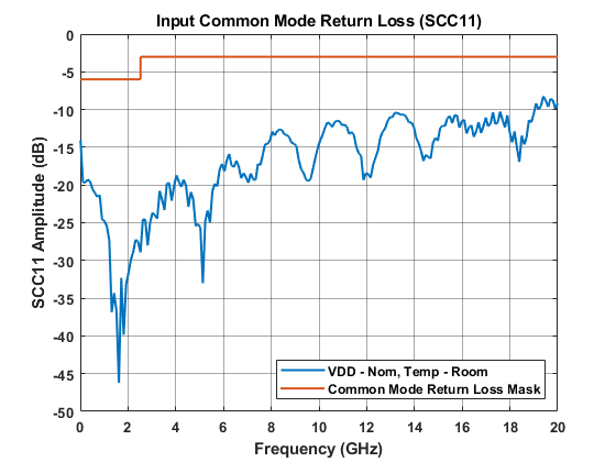 Figure 4. Typical Input (RX) Common Mode Return Loss vs Frequency in TI Evaluation Board with ~2 dB Input and ~2 dB Output Loss
 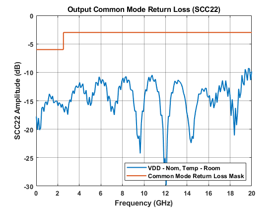 Figure 6. Typical Output (TX) Common Mode Return Loss vs Frequency in TI Evaluation Board with ~2 dB Input and ~2 dB Output Loss
 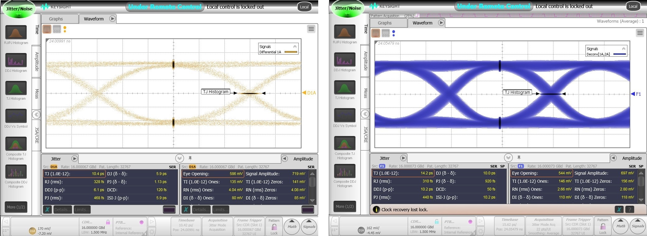 Figure 7. SN75LVPE4410 Typical Jitter Characteristics in TI Evaluation Board. Left - Input to the Device, Right - Output of the Device with Jitter Decomposition Shown.