-
SRC4190 192-kHz Stereo Asynchronous Sample-Rate Converters
- 1 Features
- 2 Applications
- 3 Description
- 4 Revision History
- 5 Pin Configuration and Functions
- 6 Specifications
- 7 Detailed Description
-
8 Application and Implementation
- 8.1 Application Information
- 8.2 Typical Application
- 9 Power Supply Recommendations
- 10Layout
- 11Device and Documentation Support
- 12Mechanical, Packaging, and Orderable Information
- IMPORTANT NOTICE
Package Options
Mechanical Data (Package|Pins)
- DB|28
Thermal pad, mechanical data (Package|Pins)
Orderable Information
SRC4190 192-kHz Stereo Asynchronous Sample-Rate Converters
1 Features
- Automatic Sensing of the Input-to-Output Sampling Ratio
- Wide Input-to-Output Sampling Range:
16:1 to 1:16 - Supports Input and Output Sampling Rates
up to 212 kHz - Dynamic Range: 128 dB (–60-dB fS Input,
BW = 20 Hz to fS / 2, A-Weighted) - THD+N: –125 dB (0-dB fS Input,
BW = 20 Hz to fS / 2) - Attenuates Sampling and Reference Clock Jitter
- High-Performance, Linear Phase Digital Filtering
- Flexible Audio Serial Ports:
- Master or Slave Mode Operation Supports I2S, Left Justified, Right Justified, and TDM Data Formats
- Supports 16-, 18-, 20-, or 24-Bit Audio Data, TDM Mode Allows Daisy Chaining of up to Eight Devices
- Supports 24-, 20-, 18-, or 16-Bit Input and Output
- All Output Data is Dithered from the Internal 28-Bit Data Path
- Low Group Delay Option for Interpolation Filter
- Soft Mute Function
- Bypass Mode
- Power-Down Mode
- Operates from a Single 3.3-V Power Supply
- Small 28-Pin SSOP Package
- Pin Compatible With the SRC4192, AD1895, and AD1896
2 Applications
- Digital Mixing Consoles
- Digital Audio Workstations
- Audio Distribution Systems
- Broadcast Studio Equipment
- High-End A/V Receivers
- General Digital Audio Processing
3 Description
The SRC4190 device is an asynchronous sample rate converter designed for professional and broadcast audio applications. The SRC4190 combines a wide input-to-output sampling ratio with outstanding dynamic range and low distortion. Input and output serial ports support standard audio formats, as well as a Time Division Multiplexed (TDM) mode. Flexible audio interfaces allow the SRC4190 to connect to a wide range of audio data converters, digital audio receivers and transmitters, and digital signal processors.
The SRC4190 is a standalone pin-programmed device, with control pins for mode, data format, mute, bypass, and low group delay functions.
The SRC4190 may be operated from a single 3.3-V power supply. A separate digital I/O supply (VIO) operates with a 1.65-V to 3.6-V supply, allowing greater flexibility when interfacing to current and future generation signal processors and logic devices. The SRC4190 is available in a 28-pin SSOP package.
Device Information(1)
| PART NUMBER | PACKAGE | BODY SIZE (NOM) |
|---|---|---|
| SRC4190 | SSOP (28) | 10.20 mm × 5.30 mm |
- For all available packages, see the orderable addendum at the end of the data sheet.
Simplified Application Diagram

4 Revision History
Changes from B Revision (September 2007) to C Revision
- Added ESD Ratings table, Feature Description section, Device Functional Modes, Application and Implementation section, Power Supply Recommendations section, Layout section, Device and Documentation Support section, and Mechanical, Packaging, and Orderable Information sectionGo
- Deleted Ordering Information table; see Package Option Addendum at the end of the data sheetGo
- Added Thermal Information tableGo
Changes from A Revision (July 2003) to B Revision
- Added U.S. patent number to note (1)Go
5 Pin Configuration and Functions
Pin Functions
| PIN | I/O | DESCRIPTION | |
|---|---|---|---|
| NAME | NO. | ||
| BCKI | 5 | Input and Output | Input port bit clock I/O |
| BCKO | 25 | Input and Output | Output port bit clock I/O |
| BYPAS | 9 | Input | ASRC bypass control input (active high) |
| DGND | 8, 21 | Ground | Digital ground |
| IFMT0 | 10 | Input | Input port data format control input |
| IFMT1 | 11 | Input | Input port data format control input |
| IFMT2 | 12 | Input | Input port data format control input |
| LGRP | 1 | Input | Low group delay control input (active high) |
| LRCKI | 6 | Input and Output | Input port left and right word clock I/O |
| LRCKO | 24 | Input and Output | Output port left and right word clock I/O |
| MODE0 | 26 | Input | Serial port mode control input |
| MODE1 | 27 | Input | Serial port mode control input |
| MODE2 | 28 | Input | Serial port mode control input |
| MUTE | 14 | Input | Output mute control input (active high) |
| NC | 3 | — | No connection |
| OFMT0 | 19 | Input | Output port data format control input |
| OFMT1 | 18 | Input | Output port data format control input |
| OWL0 | 17 | Input | Output port data word length control input |
| OWL1 | 16 | Input | Output port data word length control input |
| RCKI | 2 | Input | Reference clock input |
| RDY | 15 | Output | ASRC ready status output (active low) |
| RST | 13 | Input | Reset input (active low) |
| SDIN | 4 | Input | Audio serial data input |
| SDOUT | 23 | Output | Audio serial data output |
| TDMI | 20 | Input | TDM data input. Connect to DGND when not in use. |
| VDD | 22 | Power | Digital core supply, 3.3 V |
| VIO | 7 | Power | Digital I/O supply, 1.65 V to VDD |
6 Specifications
6.1 Absolute Maximum Ratings
over operating free-air temperature range (unless otherwise noted)(1)| MIN | MAX | UNIT | |
|---|---|---|---|
| Supply voltage, VDD | –0.3 | 4 | V |
| Supply voltage, VIO | –0.3 | 4 | V |
| Digital input voltage | –0.3 | 4 | V |
| Operating temperature | –45 | 85 | °C |
| Storage temperature, Tstg | –65 | 150 | °C |
6.2 ESD Ratings
| VALUE | UNIT | |||
|---|---|---|---|---|
| V(ESD) | Electrostatic discharge | Human-body model (HBM), per ANSI/ESDA/JEDEC JS-001(1) | ±2000 | V |
| Charged-device model (CDM), per JEDEC specification JESD22-C101(2) | ±1500 | |||
6.3 Recommended Operating Conditions
over operating free-air temperature range (unless otherwise noted)| MIN | NOM | MAX | UNIT | ||
|---|---|---|---|---|---|
| VDD | VDD supply voltage | 3 | 3.3 | 3.6 | V |
| VIO 1.8-V supply voltage | 1.65 | 1.8 | 1.95 | V | |
| VIO 3.3-V supply voltage | 3 | 3.3 | 3.6 | V | |
| Operating temperature | –45 | 85 | °C | ||
6.4 Thermal Information
| THERMAL METRIC(1) | SRC4190 | UNIT | |
|---|---|---|---|
| DB (SSOP) | |||
| 28 PINS | |||
| RθJA | Junction-to-ambient thermal resistance | 77.8 | °C/W |
| RθJC(top) | Junction-to-case (top) thermal resistance | 37.6 | °C/W |
| RθJB | Junction-to-board thermal resistance | 38.4 | °C/W |
| ψJT | Junction-to-top characterization parameter | 8.8 | °C/W |
| ψJB | Junction-to-board characterization parameter | 38.1 | °C/W |
6.5 Electrical Characteristics
TA = 25°C, VDD = 3.3 V = VIO = 3.3 V (unless otherwise noted).| PARAMETER | TEST CONDITIONS | MIN | TYP | MAX | UNIT | ||
|---|---|---|---|---|---|---|---|
| DYNAMIC PERFORMANCE(1) | |||||||
| Resolution | 24 | Bits | |||||
| fSIN | Input sampling frequency | 4 | 212 | kHz | |||
| fSOUT | Output sampling frequency | 4 | 212 | kHz | |||
| Input:Output sampling ratio | Upsampling | 1:16 | |||||
| Downsampling | 16:1 | ||||||
| Dynamic range | BW = 20 Hz to fSOUT / 2, –60-dBFS input, fIN = 1 kHz, Unweighted (add 3 dB for A‑weighted result) |
44.1 kHz:48 kHz | 125 | dB | |||
| 48 kHz:44.1 kHz | 125 | ||||||
| 48 kHz:96 kHz | 125 | ||||||
| 44.1 kHz:192 kHz | 125 | ||||||
| 96 kHz:48 kHz | 125 | ||||||
| 192 kHz:12 kHz | 125 | ||||||
| 192 kHz:32 kHz | 125 | ||||||
| 192 kHz:48 kHz | 125 | ||||||
| 32 kHz:48 kHz | 125 | ||||||
| 12 kHz:192 kHz | 125 | ||||||
| Total harmonic distortion + noise |
BW = 20 Hz to fSOUT / 2, 0-dBFS input, fIN = 1 kHz, Unweighted |
44.1 kHz:48 kHz | –125 | dB | |||
| 48 kHz:44.1 kHz | –125 | ||||||
| 48 kHz:96 kHz | –125 | ||||||
| 44.1 kHz:192 kHz | –125 | ||||||
| 96 kHz:48 kHz | –125 | ||||||
| 192 kHz:12 kHz | –125 | ||||||
| 192 kHz:32 kHz | –125 | ||||||
| 192 kHz:48 kHz | –125 | ||||||
| 32 kHz:48 kHz | –125 | ||||||
| 12 kHz:192 kHz | –125 | ||||||
| Interchannel gain mismatch | 0 | dB | |||||
| Interchannel phase deviation | 0 | ° | |||||
| Mute attenuation | 24-bit word length, A-weighted | –128 | dB | ||||
| DIGITAL INTERPOLATION FILTER | |||||||
| Passband | 0.4535 × fSIN | Hz | |||||
| Passband ripple | ±0.007 | dB | |||||
| Transition band | 0.4535 × fSIN | 0.5465 × fSIN | Hz | ||||
| Stop band | 0.5465 × fSIN | Hz | |||||
| Stop band attenuation | –125 | dB | |||||
| Normal group delay (LGRP = 0) | 102.53125 / fSIN | s | |||||
| Low group delay (LGRP = 1) | 70.53125 / fSIN | s | |||||
| DIGITAL DECIMATION FILTER | |||||||
| Passband | 0.4535 × fSOUT | Hz | |||||
| Passband ripple | ±0.008 | dB | |||||
| Transition band | 0.4535 × fSOUT | 0.5465 × fSOUT | Hz | ||||
| Stop band | 0.5465 × fSOUT | Hz | |||||
| Stop band attenuation | –125 | dB | |||||
| Group delay | 36.46875 / fSOUT | s | |||||
| DIGITAL I/O | |||||||
| VIH | High-level input voltage | 0.7 × VIO | VIO | V | |||
| VIL | Low-level input voltage | 0 | 0.3 × VIO | V | |||
| IIH | High-level input current | 0.5 | 10 | µA | |||
| IIL | Low-level input current | 0.5 | 10 | µA | |||
| VOH | High-level output voltage | IO = –4 mA | 0.8 × VIO | VIO | V | ||
| VOL | Low-level output voltage | IO = 4 mA | 0 | 0.2 × VIO | V | ||
| CIN | Input capacitance | 3 | pF | ||||
| POWER SUPPLY | |||||||
| VDD | VDD operating voltage | 3 | 3.3 | 3.6 | V | ||
| VIO | VIO operating voltage | 1.65 | 3.3 | 3.6 | |||
| IDD | VDD supply current | VDD = VIO = 3.3 V, RST = 0, No clocks, fSIN = 192 kHz, fSOUT = 192 kHz |
Power down | 100 | µA | ||
| Dynamic | 66 | mA | |||||
| IIO | VIO supply current | VDD = VIO = 3.3 V, RST = 0, No clocks, fSIN = 192 kHz, fSOUT = 192 kHz |
Power down | 100 | µA | ||
| Dynamic | 2 | mA | |||||
| PD | Power dissipation | VDD = VIO = 3.3 V, RST = 0, No clocks, fSIN = 192 kHz, fSOUT = 192 kHz |
Power down | 660 | µW | ||
| Dynamic | 225 | mW | |||||
6.6 Switching Characteristics
over operating free-air temperature range (unless otherwise noted)| PARAMETER | TEST CONDITIONS | MIN | MAX | UNIT | |
|---|---|---|---|---|---|
| REFERENCE CLOCK TIMING | |||||
| RCKI frequency(1)(2) | 128 × fSMIN | 50 | MHz | ||
| tRCKIP | RCKI period | 20 | 1 / (128 × fSMIN) | ns | |
| tRCKIH | RCKI pulse width HIGH | 0.4 × tRCKIP | ns | ||
| tRCKIL | RCKI pulse width LOW | 0.4 × tRCKIP | ns | ||
| RESET TIMING | |||||
| tRSTL | RST pulse width LOW | 500 | ns | ||
| INPUT SERIAL PORT TIMING | |||||
| tLRIS | LRCKI to BCKI setup time | 10 | ns | ||
| tSIH | BCKI pulse width HIGH | 10 | ns | ||
| tSIL | BCKI pulse width LOW | 10 | ns | ||
| tLDIS | SDIN data setup time | 10 | ns | ||
| tLDIH | SDIN data hold time | 10 | ns | ||
| OUTPUT SERIAL PORT TIMING | |||||
| tDOPD | SDOUT data delay time | 10 | ns | ||
| tDOH | SDOUT data hold time | 2 | ns | ||
| tSOH | BCKO pulsewidth HIGH | 10 | ns | ||
| tSOL | BCKO pulse width LOW | 5 | ns | ||
| TDM MODE TIMING | |||||
| tLROS | LRCKO setup time | 10 | ns | ||
| tLROH | LRCKO hold time | 10 | ns | ||
| tTDMS | TDMI data setup time | 10 | ns | ||
| tTDMH | TDMI data hold time | 10 | ns | ||
6.7 Typical Characteristics
TA = 25°C, VDD = VIO = 3.3 V (unless otherwise noted).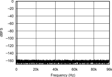 Figure 1. FFT With 1 kHz Input Tone at 0 dBFS
(12 kHz:192 kHz)
 Figure 3. FFT With 1 kHz Input Tone at 0 dBFS
(32 kHz:48 kHz)
 Figure 5. FFT With 1 kHz Input Tone at 0 dBFS
(44.1 kHz:48 kHz)
 Figure 7. FFT With 1 kHz Input Tone at 0 dBFS
(44.1 kHz:96 kHz)
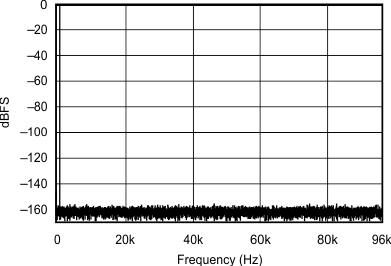 Figure 9. FFT With 1 kHz Input Tone at 0d BFS
(44.1 kHz:192 kHz)
 Figure 11. FFT With 1 kHz Input Tone at 0 dBFS
(48 kHz:44.1 kHz)
 Figure 13. FFT With 1 kHz Input Tone at 0 dBFS
(48 kHz:96 kHz)
 Figure 15. FFT With 1 kHz Input Tone at 0 dBFS
(48 kHz:192 kHz)
 Figure 17. FFT With 1 kHz Input Tone at 0 dBFS
(96 kHz:44.1 kHz)
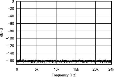 Figure 19. FFT With 1 kHz Input Tone at 0 dBFS
(96 kHz:48 kHz)
 Figure 21. FFT With 1 kHz Input Tone at 0 dBFS
(96 kHz:192 kHz)
 Figure 23. FFT With 1 kHz Input Tone at 0 dBFS
(192 kHz:12 kHz)
 Figure 25. FFT With 1 kHz Input Tone at 0 dBFS
(192 kHz:32 kHz)
 Figure 27. FFT With 1 kHz Input Tone at 0 dBFS
(192 kHz:44.1 kHz)
 Figure 29. FFT With 1 kHz Input Tone at 0 dBFS
(192 kHz:48 kHz)
 Figure 31. FFT With 1 kHz Input Tone at 0 dBFS
(192 kHz:96 kHz)
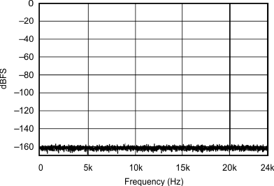 Figure 33. FFT With 20 kHz Input Tone at 0 dBFS
(44.1 kHz:48 kHz)
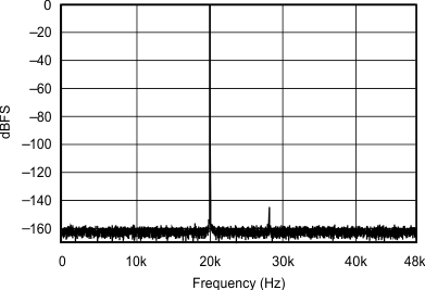 Figure 35. FFT With 20 kHz Input Tone at 0 dBFS
(48 kHz:96 kHz)
 Figure 37. FFT With 80 kHz Input Tone at 0 dBFS
(192 kHz:192 kHz)
 Figure 39. THD+N vs Input Amplitude fIN = 1 kHz
(48 kHz:44.1 kHz)
 Figure 41. THD+N vs Input Amplitude fIN = 1 kHz
(96 kHz:48 kHz)
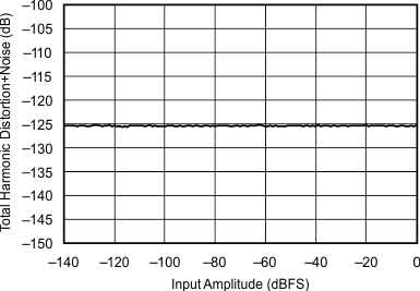 Figure 43. THD+N vs Input Amplitude fIN = 1 kHz
(192 kHz:44.1 kHz)
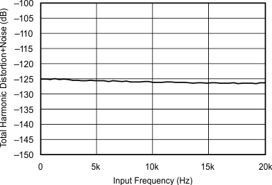 Figure 45. THD+N vs Input Frequency With
0 dBFS Input = 1 kHz (48 kHz:44.1 kHz)
 Figure 47. THD+N vs Input Frequency With 0 dBFS
(96 kHz:48 kHz)
 Figure 49. THD+N vs Input Frequency With 0 dBFS
(192 kHz:44.1 kHz)
 Figure 51. Linearity With fIN = 200 Hz (48 kHz:44.1 kHz)
 Figure 53. Linearity With fIN = 200 Hz (96 kHz:48 kHz)
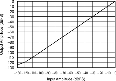 Figure 55. Linearity With fIN = 200 Hz (192 kHz:44.1 kHz)
 Figure 57. Passband Ripple (48 kHz:48 kHz)
 Figure 2. FFT With 1 kHz Input Tone at –60 dBFS
(12 kHz:192 kHz)
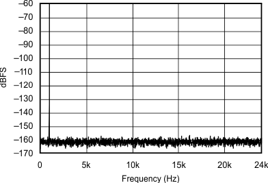 Figure 4. FFT With 1 kHz Input Tone at –60 dBFS
(32 kHz:48 kHz)
 Figure 6. FFT With 1 kHz Input Tone at –60 dBFS
(44.1 kHz:48 kHz)
 Figure 8. FFT With 1 kHz Input Tone at –60 dBFS
(44.1 kHz:96 kHz)
 Figure 10. FFT With 1 kHz Input Tone at –60 dBFS
(44.1 kHz:192 kHz)
 Figure 12. FFT With 1 kHz Input Tone at –60 dBFS
(48 kHz:44.1 kHz)
 Figure 14. FFT With 1 kHz Input Tone at –60 dBFS
(48 kHz:96 kHz)
 Figure 16. FFT With 1 kHz Input Tone at –60 dBFS
(48 kHz:192 kHz)
 Figure 18. FFT With 1 kHz Input Tone at –60 dBFS
(96 kHz:44.1 kHz)
 Figure 20. FFT With 1 kHz Input Tone at –60 dBFS
(96 kHz:48 kHz)
 Figure 22. FFT With 1 kHz Input Tone at –60 dBFS
(96 kHz:192 kHz)
 Figure 24. FFT With 1 kHz Input Tone at –60 dBFS
(192 kHz:12 kHz)
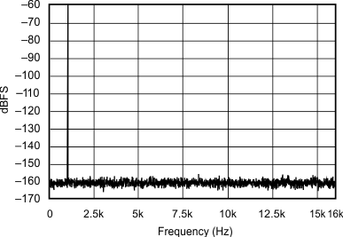 Figure 26. FFT With 1 kHz Input Tone at –60 dBFS
(192 kHz:12 kHz)
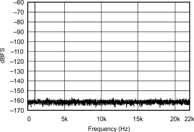 Figure 28. FFT With 1 kHz Input Tone at –60 dBFS
(192 kHz:44.1 kHz)
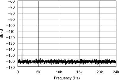 Figure 30. FFT With 1 kHz Input Tone at –60 dBFS
(192 kHz:48 kHz)
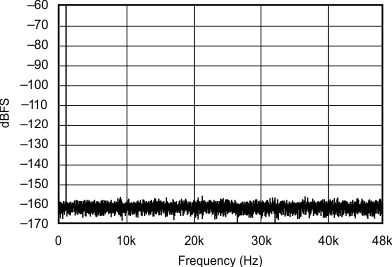 Figure 32. FFT With 1 kHz Input Tone at –60 dBFS
(192kHz:96 kHz)
 Figure 34. FFT With 20 kHz Input Tone at 0 dBFS
(48 kHz:44.1 kHz)
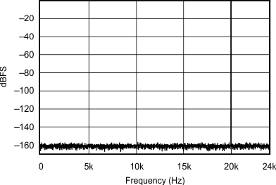 Figure 36. FFT With 20 kHz Input Tone at 0 dBFS
(96 kHz:48 kHz)
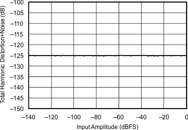 Figure 38. THD+N vs Input Amplitude fIN = 1 kHz
(44.1 kHz:48 kHz)
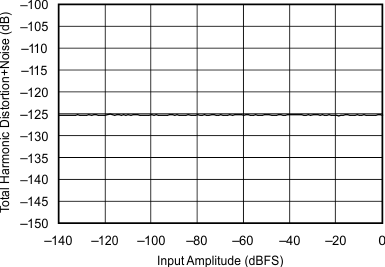 Figure 40. THD+N vs Input Amplitude fIN = 1 kHz
(48 kHz:96 kHz)
 Figure 42. THD+N vs Input Amplitude fIN = 1 kHz
(44.1 kHz:192 kHz)
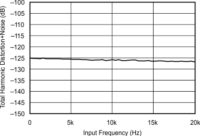 Figure 44. THD+N vs Input Frequency With 0 dBFS Input
(44.1 kHz:48 kHz)
 Figure 46. THD+N vs Input Frequency With 0 dBFS
(48 kHz:96 kHz)
 Figure 48. THD+N vs Input Frequency With 0 dBFS
(44.1 kHz:192 kHz)
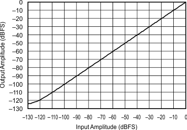 Figure 50. Linearity With fIN = 200 Hz (44.1 kHz:48 kHz)
 Figure 52. Linearity With fIN = 200 Hz (48 kHz:96 kHz)
 Figure 54. Linearity With fIN = 200 Hz (44.1 kHz:192 kHz)
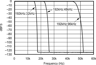 Figure 56. Frequency Response With 0 dBFS Input
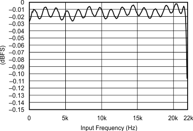 Figure 58. Passband Ripple (192 kHz:48 kHz)
7 Detailed Description
7.1 Overview
The SRC4190 device is an asynchronous sample rate converter (ASRC) designed for professional audio applications. Operation at input and output sampling frequencies up to 212 kHz is supported, with an input-to-output sampling ratio from 16:1 to 1:16. Excellent dynamic range and total harmonic distortion plus noise (THD+N) are achieved by employing high performance and linear phase digital filtering. Digital filtering options allow for lower group delay processing.
The audio input and output ports support standard audio data formats, as well as a TDM interface mode. 24-,
20-, 18-, and 16-bit word lengths are supported. Both ports may operate in slave mode, deriving their word and bit clocks from external input and output devices. Alternatively, one port may operate in master mode while the other remains in slave mode. In master mode, the LRCK and BCK clocks are derived from the reference clock input (RCKI). The flexible configuration of the input and output ports allows connection to a wide variety of audio data converters, interface devices, digital signal processors, and programmable logic.
A bypass mode is included, which allows audio data to be passed directly from the input port to the output port, bypassing the ASRC function. The bypass option is useful for passing through encoded or compressed audio data, or nonaudio control or status data.
A soft mute function is available providing artifact-free operation while muting the audio output signal. The mute attenuation is typically –128 dB.
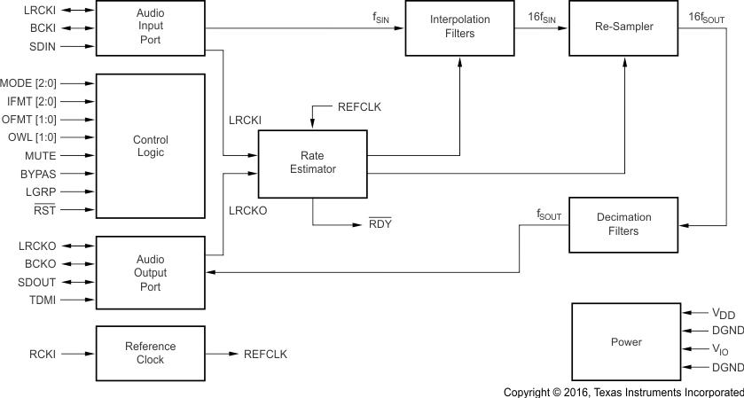
The output port data is clocked by either the audio data source in slave mode, or by the SRC4190 in master mode. The input data is passed through interpolation filters which up-sample the data, which is then passed on to the re-sampler. The rate estimator compares the input and output sampling frequencies by comparing LRCKI, LRCKO, and a reference clock. The results include an offset for the FIFO pointer and the coefficients needed for re-sampling function. The output of the re-sampler is then passed on to the decimation filter. The decimation filter performs down-sampling and anti-alias filtering functions.
7.2 Functional Block Diagram
7.3 Feature Description
7.3.1 Soft Mute Function
The soft mute function of the SRC4190 may be invoked by forcing the MUTE pin high. The soft mute function slowly attenuates the output signal level down to all zeroes plus ±4 LSB of dither. This provides an artifact-free muting of the audio output port.
7.3.2 Ready Output
The SRC4190 includes an active low ready output (RDY). This is an output from the rate estimator block, which indicates that the input-to-output sampling frequency ratio has been determined. The ready signal can be used as a flag or indicator output. The ready signal can also be connected to the active high MUTE pin to provide an auto-mute function, so that the output port is muted when the rate estimator is in transition.
7.4 Device Functional Modes
7.4.1 Bypass Mode
The SRC4190 includes a bypass function, which routes the input port data directly to the output port, bypassing the ASRC function. Bypass mode may be invoked by forcing the BYPAS pin high. For normal ASRC operation, the BYPAS pin must be set to 0.
No dithering is applied to the output data in bypass mode; digital attenuation and mute functions are also unavailable in this mode.
7.4.2 Audio Port Modes
The SRC4190 supports seven serial port modes, shown in Table 1. The audio port mode is selected using the MODE0, MODE1, and MODE2 pins.
In slave mode, the port LRCK and BCK clocks are configured as inputs, and receive their clocks from an external audio device. In master mode, the LRCK and BCK clocks are configured as outputs, being derived from the reference clock input (RCKI). Only one port can be set to master mode at any given time, as indicated in Table 1.
Table 1. Setting the Serial Port Modes
| MODE2 | MODE1 | MODE0 | SERIAL PORT MODE |
|---|---|---|---|
| 0 | 0 | 0 | Both input and output ports are slave mode |
| 0 | 0 | 1 | Output port is master mode with RCKI = 128 fS |
| 0 | 1 | 0 | Output port is master mode with RCKI = 512 fS |
| 0 | 1 | 1 | Output port is master mode with RCKI = 256 fS |
| 1 | 0 | 0 | Both input and output ports are slave mode |
| 1 | 0 | 1 | Input port is master mode with RCKI = 128 fS |
| 1 | 1 | 0 | Input port is master mode with RCKI = 512 fS |
| 1 | 1 | 1 | Input port is master mode with RCKI = 256 fS |
7.4.3 Input Port Operation
The audio input port is a three-wire synchronous serial interface that may operate in either slave or master mode. The SDIN pin 4 is the serial audio data input. Audio data is input at this pin in one of three standard audio data formats: Philips I2S, Left Justified, or Right Justified. The audio data word length may be up to 24 bits for I2S and Left Justified formats, while the Right Justified format supports 16, 18, 20, or 24-bit data. The data formats are shown in Figure 59, while critical timing parameters are shown in Figure 60 and listed in Switching Characteristics.
The bit clock is either an input or output at BCKI. In slave mode, BCKI is configured as an input pin, and may operate at rates from 32 fS to 128 fS, with a minimum of one clock cycle per data bit. In master mode, BCKI operates at a fixed rate of 64 fS.
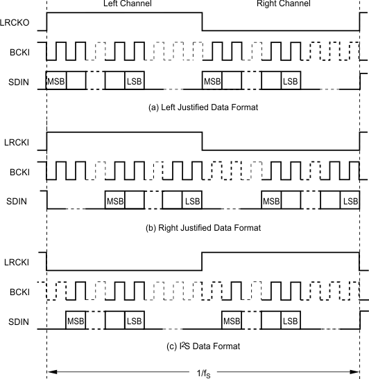 Figure 59. Input Data Formats
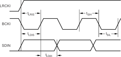 Figure 60. Input Port Timing
The left and right word clock (LRCKI), may be configured as an input or output pin. In slave mode, LRCKI is an input pin, while in master mode LRCKI is an output pin. In either case, the clock rate is equal to the input sampling frequency (fS). The LRCKI duty cycle is fixed to 50% for master mode operation. Table 2 illustrates data format selection for the input port. The IFMT0, IFMT1, and IFMT2 pins are utilized to set the input port data format.
Table 2. Input Port Data Format Selection
| IFMT2 | IMFT1 | IMFT0 | INPUT PORT DATA FORMAT |
|---|---|---|---|
| 0 | 0 | 0 | 24-Bit Left Justified |
| 0 | 0 | 1 | 24-Bit I2S |
| 0 | 1 | 0 | Unused |
| 0 | 1 | 1 | Unused |
| 1 | 0 | 0 | 16-Bit Right Justified |
| 1 | 0 | 1 | 18-Bit Right Justified |
| 1 | 1 | 0 | 20-Bit Right Justified |
| 1 | 1 | 1 | 24-Bit Right Justified |
7.4.4 Output Port Operation
The audio output port is a four-wire synchronous serial interface that may operate in either slave or master mode. The SDOUTpin is the serial audio data output. Audio data is output at this pin in one of four data formats: Philips I2S, Left Justified, Right Justified, or TDM. The audio data word length may be 16, 18, 20, or 24 bits. For all word lengths, the data is triangular PDF dithered from the internal 28-bit data path. The data formats (with the exception of TDM mode) are shown in Figure 61, while critical timing parameters are shown in Figure 62 and listed in Switching Characteristics. The TDM format and timing are shown in Figure 66 and Figure 66, respectively, while examples of standard TDM configurations are shown in Figure 69 and Figure 70. The bit clock is either input or output at BCKO. In slave mode, BCKO is configured as an input pin, and may operate at rates from 32 fS to 128 fS, with a minimum of one clock cycle for each data bit. The exception is the TDM mode, where the BCKO must operate at N × 64fS, where N is equal to the number of SRC4190 devices included on the TDM interface. In master mode, BCKO operates at a fixed rate of 64 fS for all data formats except TDM, where BCKO operates at the reference clock (RCKI) frequency. Additional information regarding TDM mode operation is included in Application and Implementation.
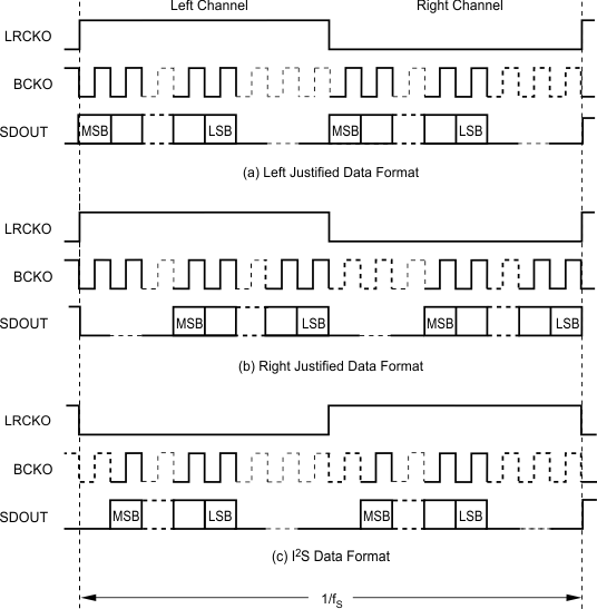 Figure 61. Output Data Formats
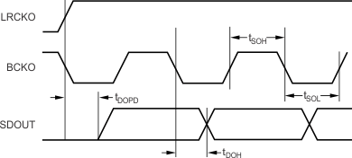 Figure 62. Output Port Timing
The left and right word clock (LRCKO), may be configured as an input or output pin. In slave mode, LRCKO is an input pin, while in master mode it is an output pin. In either case, the clock rate is equal to the output sampling frequency (fS). The clock duty cycle is fixed to 50% for I2S, Left Justified, and Right Justified formats in master mode. The LRCKO pulse width is fixed to 32 BCKO cycles for the TDM format in master mode.
Table 3 shows data format selection for the output port. The OFMT0, OFMT1, OWL0, and OWL1 inputs are utilized to set the output port data format and word length.
Table 3. Output Port Data Format Selection
| OFMT1 | OFMT0 | OUTPUT PORT DATA FORMAT |
|---|---|---|
| 0 | 0 | Left Justified |
| 0 | 1 | I2S |
| 1 | 0 | TDM |
| 1 | 1 | Right Justified |
| OWL1 | OWL2 | OUTPUT PORT DATA WORD LENGTH |
| 0 | 0 | 24 bits |
| 0 | 1 | 20 bits |
| 1 | 0 | 18 bits |
| 1 | 1 | 16 bits |
8 Application and Implementation
NOTE
Information in the following applications sections is not part of the TI component specification, and TI does not warrant its accuracy or completeness. TI’s customers are responsible for determining suitability of components for their purposes. Customers should validate and test their design implementation to confirm system functionality.
8.1 Application Information
The audio input and output ports can handle 16-, 18-, 20-, or 24-bit right-justified PCM serial data, as well as
24-bit I2S or left-justified PCM serial data at up to 212-kHz sampling rate. A TDM format is also available. Both input and output can operate in slave mode, or one can operate as a master while the other operates as a slave. A 16:1 or 1:16 ratio is the maximum supported between the input and output audio sampling rates.
8.2 Typical Application
 Figure 63. Typical Connection Diagram for the SRC4190
8.2.1 Design Requirements
For this design example, use the parameters listed in Table 4 as the input parameters.
Table 4. Design Parameters
| PARAMETER | VALUE |
|---|---|
| VDD supply voltage, VDD | 3.3 V |
| VIO supply voltage, VIO | 1.65 V to VDD |
| Bypass capacitors | 0.1 µF and 10 µF |
8.2.2 Detailed Design Procedure
The typical connection diagram for the SRC4190 is shown in Figure 63. Recommended values for power supply bypass capacitors are included. These capacitors must be placed as close to the IC package as possible.
8.2.2.1 Reference Clock
The SRC4190 requires a reference clock for operation. The reference clock is applied at the RCKI input. Figure 64 shows the reference clock connections and requirements for the SRC4190. The reference clock may operate at 128 fS, 256 fS, or 512 fS, where fS is the input or output sampling frequency. The maximum external reference clock input frequency is 50 MHz.
 Figure 64. Reference Clock Input Connections and Timing Requirements
8.2.2.2 Interfacing to Digital Audio Receivers and Transmitters
The SRC4190 input and output ports are designed to interface to a variety of audio devices, including receivers and transmitters commonly used for AES/EBU, S/PDIF, and CP1201 communications. Texas Instruments manufactures the DIR1703 digital audio interface receiver and the DIT4096 and DIT4192 digital audio transmitters to address these applications.
Figure 65 illustrates interfacing the DIR1703 to the SRC4190 input port. The DIR1703 operates from a single 3.3‑V supply, which requires the VIO supply for the SRC4190 to be set to 3.3-V for interface compatibility.
 Figure 65. Interfacing the SRC4190 to the DIR1703 Digital Audio Interface Receiver
Figure 66 shows the interface between the SRC4190 output port and the DIT4096 or DIT4192 audio serial port. Once again, the VIO supplies for both the SRC4190, DIT4096, and DIT4192 are set to 3.3 V for compatibility.
 Figure 66. Interfacing the SRC4190 to the DIT4096 and DIT4192 Digital Audio Interface Transmitter
Like the SRC4190 output port, the DIT4096 and DIT4192 audio serial port may be configured as a master or slave. In cases where the SRC4190 output port is set to master mode, TI recommends using the reference clock source (RCKI) as the master clock source (MCLK) for the DIT4096 and DIT4192, to ensure that the transmitter is synchronized to the SRC4190 output port data.
8.2.2.3 TDM Applications
The SRC4190 supports a TDM output mode, which allows multiple devices to be daisy-chained together to create a serial frame. Each device occupies one sub-frame within a frame, and each sub-frame carries two channels (Left followed by Right). Each sub-frame is 64 bits long, with 32 bits allotted for each channel. The audio data for each channel is Left Justified within the allotted 32 bits. Figure 66 illustrates the TDM frame format, while Figure 68 shows the TDM input timing parameters, which are listed in Switching Characteristics.

 Figure 68. Input Timing for TDM Mode
The frame rate is equal to the output sampling frequency. The BCKO frequency for the TDM interface is
N × 64 fS, where N is the number of devices included in the daisy chain. For master mode, the output BCKO frequency is fixed to the reference clock (RCKI) input frequency. The number of devices that can be daisy-chained in TDM mode is dependent upon the output sampling frequency and the BCKO frequency, leading to the numerical relationship in Equation 1
where
- fBCKO = Output port bit clock (BCKO) (27.136-MHz maximum)
- fS = Output port sampling (LRCKO) frequency (212-kHz maximum)
This relationship holds true for both slave and master modes. Figure 69 and Figure 70 show typical connection schemes for the TDM mode. Although the TMS320C671x DSP family is shown as the audio processing engine in these figures, other TI digital signal processors with a multi-channel buffered serial port (McBSPTM) may also function with this arrangement. Interfacing to processors from other manufacturers is also possible. See Figure 62, along with the equivalent serial port timing diagrams shown in the DSP data sheet, to determine compatibility.
 Figure 69. TDM Interface With All Devices as Slaves
 Figure 70. TDM Interface With One Device as Master to Multiple Slaves
8.2.2.4 Pin Compatibility With the Analog Devices AD1895 and AD1896
The SRC4190 is pin and function-compatible with the AD1895 and AD1896 when observing the guidelines indicated in the following paragraphs.
8.2.2.4.1 Power Supplies
To ensure compatibility, the VDD_IO and VDD_CORE supplies of the AD1895 and AD1896 must be set to 3.3 V, while the VIO and VDD supplies of the SRC4190 must be set to 3.3 V.
8.2.2.4.2 Pin 1 Connection
For the AD1895, pin 1 is not connected. For the SRC4190, pin 1 (LGRP) functions as the low group delay selection input, and must not be left unconnected. LGRP must be connected to either digital ground or the VIO supply, dependent upon the desired group delay.
8.2.2.4.3 Crystal Oscillator
The SRC4190 does not have an on-chip crystal oscillator. An external reference clock is required at the RCKI pin.
8.2.2.4.4 Reference Clock Frequency
The reference clock input frequency for the SRC4190 must be no higher than 30 MHz, in order to match the master clock frequency specification of the AD1895 and AD1896. In addition, the SRC4190 does not support the 768-fS reference clock rate.
8.2.2.4.5 Master Mode Maximum Sampling Frequency
When the input or output ports are set to master mode, the maximum sampling frequency must be limited to
96 kHz in order to support the AD1895 and AD1896 specification. This is despite the fact that the SRC4190 supports a maximum sampling frequency of 212 kHz in master mode. The user must consider building an option into his or her design to support the higher sampling frequency of the SRC4190.
8.2.2.4.6 Matched Phase Mode
Due to the internal architecture of the SRC4190, it does not require or support the matched phase mode of the AD1896. Given multiple SRC4190 devices, if all reference clock (RCKI) inputs are driven from the same clock source, the devices is phase matched.
8.2.3 Application Curves
 Figure 71. FFT With 1 kHz Input Tone at –60 dBFS
(44.1 kHz:48 kHz)
 Figure 72. FFT With 1 kHz Input Tone at –60 dBFS
(44.1 kHz:96 kHz)