SLASF30 January 2022 TAA5212
ADVANCE INFORMATION
- 1
- 1 Features
- 2 Applications
- 3 Description
- 4 Revision History
- 5 Pin Configuration and Functions
-
6 Specifications
- 6.1 Absolute Maximum Ratings
- 6.2 ESD Ratings
- 6.3 Recommended Operating Conditions
- 6.4 Thermal Information
- 6.5 Electrical Characteristics
- 6.6 Timing Requirements: I2C Interface
- 6.7 Switching Characteristics: I2C Interface
- 6.8 Timing Requirements: SPI Interface
- 6.9 Switching Characteristics: SPI Interface
- 6.10 Timing Requirements: TDM, I2S or LJ Interface
- 6.11 Switching Characteristics: TDM, I2S or LJ Interface
- 6.12 Timing Requirements: PDM Digital Microphone Interface
- 6.13 Switching Characteristics: PDM Digial Microphone Interface
- 7 Parameter Measurement Information
-
8 Detailed Description
- 8.1 Overview
- 8.2 Functional Block Diagram
- 8.3
Feature Description
- 8.3.1 Hardware Control
- 8.3.2 Serial Interfaces
- 8.3.3 Phase-Locked Loop (PLL) and Clock Generation
- 8.3.4 Input Channel Configurations
- 8.3.5 Reference Voltage
- 8.3.6 Programmable Microphone Bias
- 8.3.7
Signal-Chain Processing
- 8.3.7.1
ADC Signal-Chain
- 8.3.7.1.1 Programmable Channel Gain and Digital Volume Control
- 8.3.7.1.2 Programmable Channel Gain Calibration
- 8.3.7.1.3 Programmable Channel Phase Calibration
- 8.3.7.1.4 Programmable Digital High-Pass Filter
- 8.3.7.1.5 Programmable Digital Biquad Filters
- 8.3.7.1.6 Programmable Channel Summer and Digital Mixer
- 8.3.7.1.7 Configurable Digital Decimation Filters
- 8.3.7.1
ADC Signal-Chain
- 8.3.8 Interrupts, Status, and Digital I/O Pin Multiplexing
- 8.3.9 Programmable Channel Phase Calibration
- 8.4 Device Functional Modes
- 8.5 Register Maps
- 8.6 Feature Description
- 8.7 Device Functional Modes
- 9 Application and Implementation
- 10Power Supply Recommendations
- 11Layout
- 12Device and Documentation Support
- 13Mechanical, Packaging, and Orderable Information
Package Options
Mechanical Data (Package|Pins)
- RGE|24
Thermal pad, mechanical data (Package|Pins)
- RGE|24
Orderable Information
8.3.7.1.6 Programmable Channel Summer and Digital Mixer
For applications that require an even higher SNR than that supported for each channel, the device digital summing mode can be used. In this mode, the digital record data are summed up across the channel with an equal weightage factor, which helps in reducing the effective record noise.
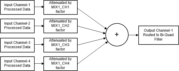
The device supports a fully programmable mixer feature that can mix the various input channels with their custom programmable scale factor to generate the final output channels. Figure 8-19 shows a block diagram that describes the mixer 1 operation to generate output channel 1.
 Figure 8-19 Programmable Digital Mixer Block Diagram
A similar mixer operation is performed by mixer 2, mixer 3, and mixer 4 to generate output channel 2, channel 3, and channel 4, respectively.