SLASE86E June 2016 – December 2017 TAS2560
PRODUCTION DATA.
- 1 Features
- 2 Applications
- 3 Description
- 4 Revision History
- 5 Device Comparison Table
- 6 Pin Configuration and Functions
-
7 Specifications
- 7.1 Absolute Maximum Ratings
- 7.2 ESD Ratings
- 7.3 Recommended Operating Conditions
- 7.4 Thermal Information
- 7.5 Electrical Characteristics
- 7.6 I2C Timing Requirements
- 7.7 I2S/LJF/RJF Timing in Master Mode
- 7.8 I2S/LJF/RJF Timing in Slave Mode
- 7.9 DSP Timing in Master Mode
- 7.10 DSP Timing in Slave Mode
- 7.11 PDM Timing
- 7.12 Typical Characteristics
- 8 Parameter Measurement Information
-
9 Detailed Description
- 9.1 Overview
- 9.2 Functional Block Diagram
- 9.3
Feature Description
- 9.3.1 General I2C Operation
- 9.3.2 Single-Byte and Multiple-Byte Transfers
- 9.3.3 Single-Byte Write
- 9.3.4 Multiple-Byte Write and Incremental Multiple-Byte Write
- 9.3.5 Single-Byte Read
- 9.3.6 Multiple-Byte Read
- 9.3.7 PLL
- 9.3.8 Clock Distribution
- 9.3.9 Clock Error Detection
- 9.3.10 Class-D Edge Rate Control
- 9.3.11 IV Sense
- 9.3.12 Boost Control
- 9.3.13 Thermal Fold-back
- 9.3.14 Battery Guard AGC
- 9.3.15 Configurable Boost Current Limit (ILIM)
- 9.3.16 Fault Protection
- 9.3.17 Spread Spectrum vs Synchronized
- 9.3.18 IRQs and Flags
- 9.3.19 CRC checksum for I2C
- 9.3.20 PurePath Console 3 Software TAS2560 Application
- 9.4 Device Functional Modes
- 9.5 Operational Modes
- 9.6 Programming
- 9.7
Register Map
- 9.7.1 Register Map Summary
- 9.7.2 PAGE (book=0x00 page=0x00 address=0x00) [reset=0h]
- 9.7.3 RESET (book=0x00 page=0x00 address=0x01) [reset=0h]
- 9.7.4 MODE (book=0x00 page=0x00 address=0x02) [reset=1h]
- 9.7.5 SPK_CTRL (book=0x00 page=0x00 address=0x04) [reset=5Fh]
- 9.7.6 PWR_CTRL_2 (book=0x00 page=0x00 address=0x05) [reset=0h]
- 9.7.7 PWR_CTRL_1 (book=0x00 page=0x00 address=0x07) [reset=0h]
- 9.7.8 RAMP_CTRL (book=0x00 page=0x00 address=0x08) [reset=1h]
- 9.7.9 EDGE_ISNS_BOOST (book=0x00 page=0x00 address=0x09) [reset=83h]
- 9.7.10 PLL_CLKIN (book=0x00 page=0x00 address=0x0F) [reset=41h]
- 9.7.11 PLL_JVAL (book=0x00 page=0x00 address=0x10) [reset=4h]
- 9.7.12 PLL_DVAL_1 (book=0x00 page=0x00 address=0x11) [reset=0h]
- 9.7.13 PLL_DVAL_2 (book=0x00 page=0x00 address=0x12) [reset=0h]
- 9.7.14 ASI_FORMAT (book=0x00 page=0x00 address=0x14) [reset=2h]
- 9.7.15 ASI_CHANNEL (book=0x00 page=0x00 address=0x15) [reset=0h]
- 9.7.16 ASI_OFFSET_1 (book=0x00 page=0x00 address=0x16) [reset=0h]
- 9.7.17 ASI_OFFSET_2 (book=0x00 page=0x00 address=0x17) [reset=0h]
- 9.7.18 ASI_CFG_1 (book=0x00 page=0x00 address=0x18) [reset=0h]
- 9.7.19 ASI_DIV_SRC (book=0x00 page=0x00 address=0x19) [reset=0h]
- 9.7.20 ASI_BDIV (book=0x00 page=0x00 address=0x1A) [reset=1h]
- 9.7.21 ASI_WDIV (book=0x00 page=0x00 address=0x1B) [reset=40h]
- 9.7.22 PDM_CFG (book=0x00 page=0x00 address=0x1C) [reset=0h]
- 9.7.23 PDM_DIV (book=0x00 page=0x00 address=0x1D) [reset=8h]
- 9.7.24 DSD_DIV (book=0x00 page=0x00 address=0x1E) [reset=8h]
- 9.7.25 CLK_ERR_1 (book=0x00 page=0x00 address=0x21) [reset=3h]
- 9.7.26 CLK_ERR_2 (book=0x00 page=0x00 address=0x22) [reset=3Fh]
- 9.7.27 IRQ_PIN_CFG (book=0x00 page=0x00 address=0x23) [reset=21h]
- 9.7.28 INT_CFG_1 (book=0x00 page=0x00 address=0x24) [reset=0h]
- 9.7.29 INT_CFG_2 (book=0x00 page=0x00 address=0x25) [reset=0h]
- 9.7.30 INT_DET_1 (book=0x00 page=0x00 address=0x26) [reset=0h]
- 9.7.31 INT_DET_2 (book=0x00 page=0x00 address=0x27) [reset=0h]
- 9.7.32 STATUS_POWER (book=0x00 page=0x00 address=0x2A) [reset=0h]
- 9.7.33 SAR_VBAT_MSB (book=0x00 page=0x00 address=0x2D) [reset=C0h]
- 9.7.34 SAR_VBAT_LSB (book=0x00 page=0x00 address=0x2E) [reset=0h]
- 9.7.35 DIE_TEMP_SENSOR (book=0x00 page=0x00 address=0x31) [reset=0h]
- 9.7.36 LOW_PWR_MODE (book=0x00 page=0x00 address=0x35) [reset=0h]
- 9.7.37 PCM_RATE (book=0x00 page=0x00 address=0x36) [reset=32h]
- 9.7.38 CLOCK_ERR_CFG_1 (book=0x00 page=0x00 address=0x4F) [reset=0h]
- 9.7.39 CLOCK_ERR_CFG_2 (book=0x00 page=0x00 address=0x50) [reset=11h]
- 9.7.40 PROTECTION_CFG_1 (book=0x00 page=0x00 address=0x58) [reset=3h]
- 9.7.41 CRC_CHECKSUM (book=0x00 page=0x00 address=0x7E) [reset=0h]
- 9.7.42 BOOK (book=0x00 page=0x00 address=0x7F) [reset=0h]
- 10Application and Implementation
- 11Power Supply Recommendations
- 12Layout
- 13Device and Documentation Support
- 14Mechanical, Packaging, and Orderable Information
Package Options
Refer to the PDF data sheet for device specific package drawings
Mechanical Data (Package|Pins)
- YFF|30
Thermal pad, mechanical data (Package|Pins)
Orderable Information
8 Parameter Measurement Information
 Figure 23. TAS2560 Test Circuit
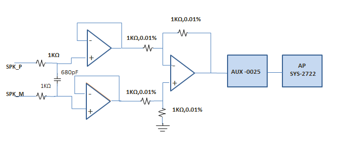
All typical characteristics for the devices are measured using the bench EVM and an Audio Precision SYS-2722 audio analyzer. A Programable Serial Interface Adaptor (PSIA) is used to allow the I2S interface to be driven directly into the SYS-2722. SPEAKER OUT terminal is connected to Audio Precision analyzer inputs as shown below. There is a differential to single ended (D2S) filter, with 1st order Passive pole at 120 kHz is added. This is to ensure high performance Class-D amplifier sees a fully differential matched loading at its outputs and no degradation in performance measured due to loading effects of AUX filter on Class-D outputs.
 Figure 24. Differential To Single Ended (D2S) Filter