SLOSE43A April   2020  – July 2020 TAS5431-Q1

PRODUCTION DATA  

  1. Features
  2. Applications
  3. Description
  4. Revision History
  5. Pin Configuration and Functions
    1.     Pin Functions
  6. Specifications
    1. 6.1 Absolute Maximum Ratings
    2. 6.2 ESD Ratings
    3. 6.3 Recommended Operating Conditions
    4. 6.4 Thermal Information
    5. 6.5 Electrical Characteristics
    6. 6.6 Timing Requirements for I2C Interface Signals
    7. 6.7 Typical Characteristics
  7. Detailed Description
    1. 7.1 Overview
    2. 7.2 Functional Block Diagram
    3. 7.3 Feature Description
      1. 7.3.1 Analog Audio Input and Preamplifier
      2. 7.3.2 Pulse-Width Modulator (PWM)
      3. 7.3.3 Gate Drive
      4. 7.3.4 Power FETs
      5. 7.3.5 Load Diagnostics
        1. 7.3.5.1 Load Diagnostics Sequence
        2. 7.3.5.2 Faults During Load Diagnostics
      6. 7.3.6 Protection and Monitoring
      7. 7.3.7 I2C Serial Communication Bus
        1. 7.3.7.1 I2C Bus Protocol
        2. 7.3.7.2 Random Write
        3. 7.3.7.3 Random Read
        4. 7.3.7.4 Sequential Read
    4. 7.4 Device Functional Modes
      1. 7.4.1 Hardware Control Pins
      2. 7.4.2 EMI Considerations
      3. 7.4.3 Operating Modes and Faults
    5. 7.5 Register Maps
      1. 7.5.1 I2C Address Register Definitions
  8. Application and Implementation
    1. 8.1 Application Information
    2. 8.2 Typical Application
      1. 8.2.1 Design Requirements
        1. 8.2.1.1 Amplifier Output Filtering
        2. 8.2.1.2 Amplifier Output Snubbers
        3. 8.2.1.3 Bootstrap Capacitors
        4. 8.2.1.4 Analog Audio Input Filter
      2. 8.2.2 Detailed Design Procedure
        1. 8.2.2.1 Unused Pin Connections
          1. 8.2.2.1.1 MUTE Pin
          2. 8.2.2.1.2 STANDBY Pin
          3. 8.2.2.1.3 I2C Pins (SDA and SCL)
          4. 8.2.2.1.4 Terminating Unused Outputs
          5. 8.2.2.1.5 Using a Single-Ended Audio Input
      3. 8.2.3 Application Curves
  9. Power Supply Recommendations
  10. 10Layout
    1. 10.1 Layout Guidelines
    2. 10.2 Layout Examples
      1. 10.2.1 Top Layer
      2. 10.2.2 Second Layer – Signal Layer
      3. 10.2.3 Third Layer – Power Layer
      4. 10.2.4 Bottom Layer – Ground Layer
  11. 11Device and Documentation Support
    1. 11.1 Device Support
      1. 11.1.1 Third-Party Products Disclaimer
    2. 11.2 Documentation Support
      1. 11.2.1 Related Documentation
    3. 11.3 Receiving Notification of Documentation Updates
    4. 11.4 Support Resources
    5. 11.5 Trademarks
    6. 11.6 Electrostatic Discharge Caution
    7. 11.7 Glossary
  12. 12Mechanical, Packaging, and Orderable Information

Package Options

Mechanical Data (Package|Pins)
Thermal pad, mechanical data (Package|Pins)
Orderable Information

Description

The TAS5431-Q1 is a mono class-D audio amplifier, ideal for use in automotive emergency call (eCall), telematics, instrument cluster, and infotainment applications. The device provides up to 8-W into 4 Ω at less than 10% THD+N from a 14.4-Vdc automotive battery. The wide operating voltage range and excellent efficiency make the device ideal for start-stop support or running from a backup battery when required. The integrated load-dump protection reduces external voltage clamp cost and size, and the onboard load diagnostics report the status of the speaker through I2C.

Device Information
PART NUMBER PACKAGE(1) BODY SIZE (NOM)
TAS5431-Q1 HTSSOP (16) 5.00 mm × 4.40 mm
For all available packages, see the orderable addendum at the end of the datasheet.
GUID-95C579C1-09BE-412F-B15A-FDE19B09FCFF-low.gif Simplified Block Diagram
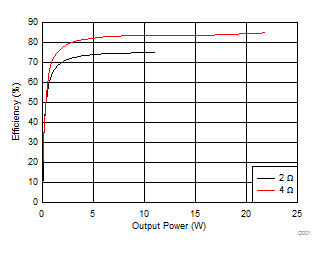
GUID-DB373965-D3CC-4A3C-B70A-E32B5951C90F-low.gif Output Power Efficiency