SLAS846A May 2012 – March 2015 TAS5614LA
PRODUCTION DATA.
- 1 Features
- 2 Applications
- 3 Description
- 4 Revision History
- 5 Pin Configuration and Functions
- 6 Specifications
-
7 Detailed Description
- 7.1 Overview
- 7.2 Functional Block Diagrams
- 7.3
Feature Description
- 7.3.1 Power Supplies
- 7.3.2 System Power-Up and Power-Down Sequence
- 7.3.3 Start-up and Shutdown Ramp Sequence
- 7.3.4 Unused Output Channels
- 7.3.5 Device Protection System
- 7.3.6 Pin-to-Pin Short-Circuit Protection (PPSC)
- 7.3.7 Overtemperature Protection
- 7.3.8 Overtemperature Warning, OTW
- 7.3.9 Undervoltage Protection (UVP) and Power-On Reset (POR)
- 7.3.10 Error Reporting
- 7.3.11 Fault Handling
- 7.3.12 Device Reset
- 7.4 Device Functional Modes
- 8 Application and Implementation
- 9 Power Supply Recommendations
- 10Layout
- 11Device and Documentation Support
- 12Mechanical, Packaging, and Orderable Information
Package Options
Mechanical Data (Package|Pins)
- DDV|44
Thermal pad, mechanical data (Package|Pins)
- DDV|44
Orderable Information
8 Application and Implementation
NOTE
Information in the following applications sections is not part of the TI component specification, and TI does not warrant its accuracy or completeness. TI’s customers are responsible for determining suitability of components for their purposes. Customers should validate and test their design implementation to confirm system functionality.
8.1 Application Information
8.1.1 System Design Consideration
A rising-edge transition on reset input allows the device to execute the startup sequence and starts switching.
Apply audio only according to the timing information for startup and shutdown sequence. That will start and stop the amplifier without audible artifacts in the output transducers.
The CLIP signal indicates that the output is approaching clipping (when output PWM starts skipping pulses due to loop filter saturation). The signal can be used to initiate an audio volume decrease or to adjust the power supply rail.
The device inverts the audio signal from input to output.
The DVDD and AVDD pins are not recommended to be used as a voltage source for external circuitry.
8.2 Typical Applications
The following sections discuss in detail three typical audio PWM (class-D) configurations:
- Differential input, stereo BTL outputs
- Differential input, mono PBTL output
- Single-ended inputs, quad single-ended outputs.
8.2.1 Typical BTL Application
 Figure 16. Typical Differential (2N) BTL Application With AD Modulation Filters
8.2.1.1 Design Requirements
See Figure 16 for application schematic. In this application, differential PWM inputs are used with AD modulation from the PWM modulator (TAS5558). AD modulation scheme is defined as PWM(+) is opposite polarity from PWM(-).
8.2.1.2 Detailed Design Procedure
- Pin 1 - GVDD_AB is the gate drive voltage for half-bridges A and B. This pin needs a 3.3-Ω isolation resistor and a 0.1-uF decoupling capacitor.
- Pin 2 - VDD is the supply for internal voltage regulators AVDD and DVDD. This pin needs a 10-uF bulk capacitor and a 0.1-uF decoupling capacitor.
- Pin 3 - Roc adjust is the overcurrent programming resistor. Depending on the application, this resistor can be between 24 kΩ to 68 kΩ.
- Pin 4 - RESET pin when asserted, it keeps outputs Hi-Z and no PWM switching. This pin can be controlled by a microprocessor.
- Pins 5 and 6 - These are PWM (+) and PWM (–) pins with signals provided by a PWM modulator such as TAS5558. These are PWM differential pair.
- Pin 7 - Start-up ramp capacitor should be 0.1 uF for BTL configuration.
- Pin 8 - Digital output supply pin is connected to 1-uF decoupling capacitor.
- Pins 9-12 - Ground pins are connected to board ground.
- Pin 13 - Analog output supply pin is connected to 1-uF decoupling capacitor.
- Pins 14 and 15 - These are PWM (+) and PWM (–) pins with signals provided by a PWM modulator such as TAS5558. These are PWM differential pair.
- Pin 16 - Fault pin can be monitored by a micro-controller via GPIO pin. System can decide to assert reset or shutdown.
- Pin 17 - Overtemperature warning pin can be monitored by a microcontroller through a GPIO pin. System can decide to turn on fan or lower output power.
- Pin 18 - Output clip indicator can be monitored by a microcontroller via a GPIO pin. System can decide to lower the volume.
- Pins 19-21 - Mode pins set the input and output configurations. For this configuration M1-M3 are grounded. These mode pins must be hardware configured, such as, not through GPIO pins from a micro-controller.
- Pin 22 - GVDD_CD is the gate drive voltage for half-bridges C and D. This pin needs a 3.3-Ω isolation resistor and a 0.1-uF decoupling capacitor.
- Pins 23, 24, 43, 44 - Bootstrap pins for half-bridges A, B, C, and D. Connect 33 nF from this pin to corresponding output pins.
- Pins 25, 26, 33, 34, 41, 42 - These ground pins should be used to ground decoupling capacitors from PVDD_X.
- Pins 27, 28, 32, 35, 39, 40 - Output pins from half-bridges A, B, C, and D. Connect appropriate bootstrap capacitors and differential LC filter as shown in Figure 16.
- Pins 29, 30, 31, 36, 37, 38 - Power supply pins to half-bridges A, B, C, and D. A and B form a full-bridge and C and D form another full-bridge. A 470-uF bulk capacitor is recommended for each full-bridge power pins. Two 0.22-µF decoupling capacitors are placed on each full-bridge power pins. See Figure 16 for details.
8.2.1.3 Application Curves
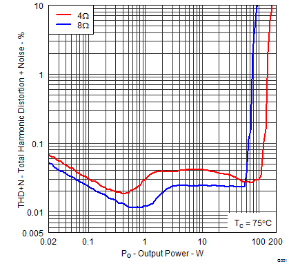 Figure 17. Total Harmonic + Noise vs Output Power, 1 kHz
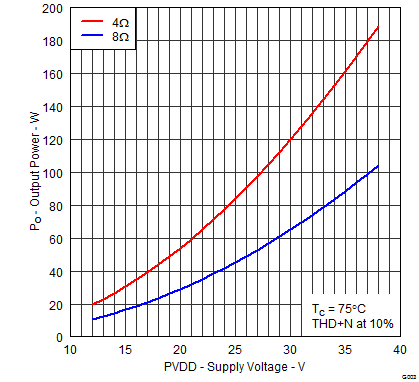 Figure 18. Output Power vs Supply Voltage vs Distortion + Noise = 10%
8.2.2 Typical SE Configuration
 Figure 19. Typical (1N) SE Application
8.2.2.1 Design Requirements
See Figure 19 for application schematic. In this application, four single-ended PWM inputs are used with AD modulation from the PWM modulator such as the TAS5558. AD modulation scheme is defined as PWM(+) is opposite polarity from PWM(-). The single-ended (SE) output configuration is often used to drive 4 independent channels in one TAS5614LA device.
8.2.2.2 Detailed Design Procedure
- Pin 1 - GVDD_AB is the gate drive voltage for half-bridges A and B. It needs a 3.3-Ω isolation resistor and a 0.1-uF decoupling capacitor.
- Pin 2 - VDD is the supply for internal voltage regulators AVDD and DVDD. It needs a 10-uF bulk cap and a 0.1-uF decoupling capacitor.
- Pin 3 - Roc adjust is the overcurrent programming resistor. Depending on the application, this resistor can be between 24 kΩ to 68 kΩ.
- Pin 4 - RESET pin when asserted, it keeps outputs Hi-Z and no PWM switching. This pin can be controlled by a microprocessor.
- Pins 5 and 6 - These are PWM (+) and PWM (–) pins with signals provided by a PWM modulator such as TAS5558. These are PWM differential pair.
- Pin 7 - Start up ramp capacitor should be 1 uF for SE configuration.
- Pin 8 - Digital output supply pin is connected to 1-uF decoupling cap.
- Pins 9-12 - Ground pins are connected to board ground.
- Pin 13 - Analog output supply pin is connected to 1-uF decoupling cap.
- Pins 14 and 15 - These are PWM (+) and PWM (–) pins with signals provided by a PWM modulator such as TAS5558. These are PWM differential pair.
- Pin 16 - Fault pin can be monitored by a microcontroller through GPIO pin. System can decide to assert reset or shutdown.
- Pin 17 - Overtemperature warning pin can be monitored by a microcontroller through a GPIO pin. System can decide to turn on fan or lower output power.
- Pin 18 - Output clip indicator can be monitored by a microcontroller through a GPIO pin. System can decide to lower the volume.
- Pins 19-21 - Mode pins set the input and output configurations. For this configuration M1-M3 are grounded. These mode pins must be hardware configured, such as, not through GPIO pins from a microcontroller.
- Pin 22 - GVDD_CD is the gate drive voltage for half-bridges C and D. This pin needs a 3.3-Ω isolation resistor and a 0.1-uF decoupling capacitor.
- Pins 23, 24, 43, 44 - Bootstrap pins for half-bridges A, B, C, and D. Connect 33 nF from this pin to corresponding output pins.
- Pins 25, 26, 33, 34, 41, 42 - These ground pins should be used to ground decoupling capacitors from PVDD_X.
- Pins 27, 28, 32, 35, 39, 40 - Output pins from half-bridges A, B, C, and D. Connect appropriate bootstrap capacitors and differential LC filter as shown in Figure 19.
- Pins 29, 30, 31, 36, 37, 38 - Power supply pins to half-bridges A, B, C, and D. A and B form a full-bridge and C and D form another full-bridge. A 470-uF bulk cap is recommended for each full-bridge power pins. Two 0.22-µF decoupling capacitors are placed on each full-bridge power pins. See Figure 19 for details.
8.2.2.3 Application Curves
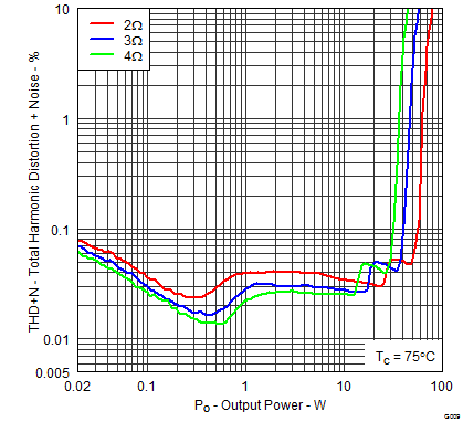 Figure 20. Total Harmonic Distortion + Noise vs Output Power
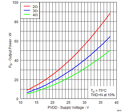 Figure 21. Output Power vs Supply Voltage
8.2.3 Typical PBTL Configuration
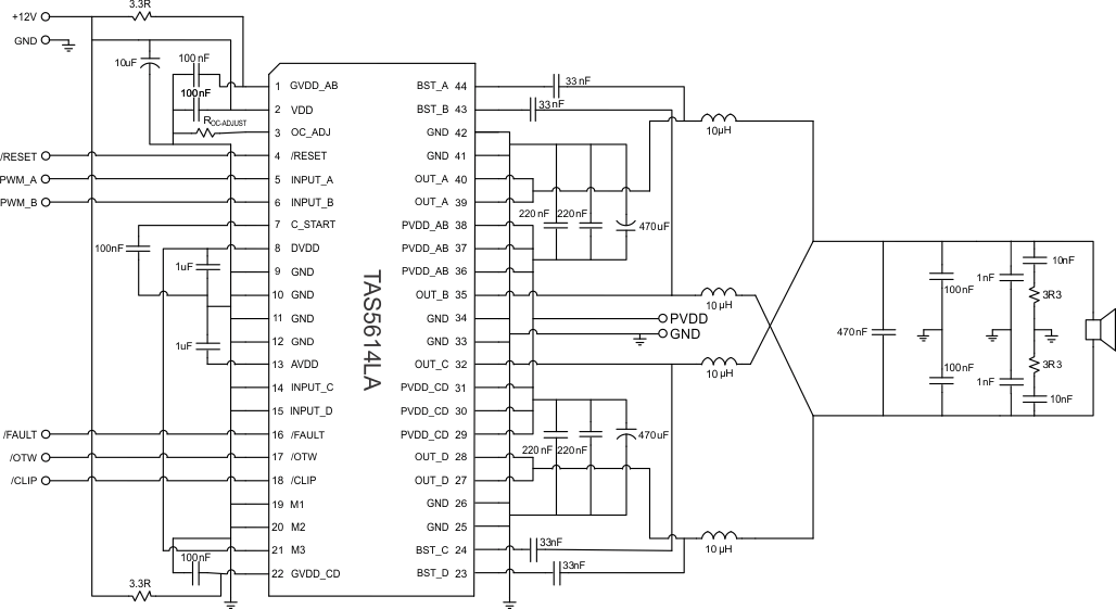 Figure 22. Typical Differential (2N) PBTL Application With AD Modulation Filter
8.2.3.1 Design Requirements
See Figure 22 for application schematic. In this application, one differential PWM input is used with AD modulation from the PWM modulator such as the TAS5558. AD modulation scheme is defined as PWM(+) is opposite polarity from PWM(-). The output PBTL configuration is often used to drive lower impedance load such as a subwoofer.
8.2.3.2 Detailed Design Procedure
- Pin 1 - GVDD_AB is the gate drive voltage for half-bridges A and B. This pin needs a 3.3-Ω isolation resistor and a 0.1-uF decoupling capacitor.
- Pin 2 - VDD is the supply for internal voltage regulators AVDD and DVDD. This pin needs a 10-uF bulk cap and a 0.1-uF decoupling capacitor.
- Pin 3 - Roc adjust is the over-current programming resistor. Depending on the application, this resistor can be between 24 kΩ to 68 kΩ.
- Pin 4 - RESET pin when asserted, it keeps outputs Hi-Z and no PWM switching. This pin can be controlled by a microprocessor.
- Pins 5 and 6 - These are PWM (+) and PWM (–) pins with signals provided by a PWM modulator such as TAS5558. These are PWM differential pair.
- Pin 7 - Start up ramp capacitor should be 0.1 uF for PBTL configuration.
- Pin 8 - Digital output supply pin is connected to 1-uF decoupling capacitor.
- Pins 9-12 - Ground pins are connected to board ground.
- Pin 13 - Analog output supply pin is connected to 1-uF decoupling cap.
- Pins 14 and 15 - These are PWM (+) and PWM (–) pins with signals provided by a PWM modulator such as TAS5558. These are PWM differential pair.
- Pin 16 - Fault pin can be monitored by a microcontroller through GPIO pin. System can decide to assert reset or shutdown.
- Pin 17 - Overtemperature warning pin can be monitored by a microcontroller through a GPIO pin. System can decide to turn on fan or lower output power.
- Pin 18 - Output clip indicator can be monitored by a microcontroller through a GPIO pin. System can decide to lower the volume.
- Pins 19-21 - Mode pins set the input and output configurations. For this configuration M1-M3 are grounded. These mode pins must be hardware configured, such as, not through GPIO pins from a microcontroller.
- Pin 22 - GVDD_CD is the gate drive voltage for half-bridges C and D. It needs a 3.3-Ω isolation resistor and a 0.1-uF decoupling capacitor.
- Pins 23, 24, 43, 44 - Bootstrap pins for half-bridges A, B, C, and D. Connect 33 nF from this pin to corresponding output pins.
- Pins 25, 26, 33, 34, 41, 42 - These ground pins should be used to ground decoupling capacitors from PVDD_X.
- Pins 27, 28, 32, 35, 39, 40 - Output pins from half-bridges A, B, C, and D. Connect appropriate bootstrap capacitors and differential LC filter as shown in Figure 22.
- Pins 29, 30, 31, 36, 37, 38 - Power supply pins to half-bridges A, B, C, and D. A and B form a full-bridge and C and D form another full-bridge. A 470-uF bulk cap is recommended for each full-bridge power pins. Two 0.22-µF decoupling capacitors are placed on each full-bridge power pins. See Figure 22 for details.
8.2.3.3 Application Curves
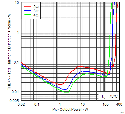 Figure 23. Total Harmonic Distortion + Noise vs Output Power
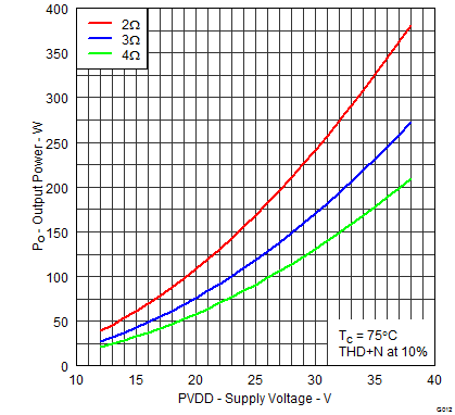 Figure 24. Output Power vs Supply Voltage