SLES217D November 2010 – March 2015 TAS5630B
PRODUCTION DATA.
- 1 Features
- 2 Applications
- 3 Description
- 4 Revision History
- 5 Pin Configuration and Functions
- 6 Specifications
-
7 Detailed Description
- 7.1 Overview
- 7.2 Functional Block Diagram
- 7.3
Feature Description
- 7.3.1 Power Supplies
- 7.3.2 System Power-Up and Power-Down Sequence
- 7.3.3 Error Reporting
- 7.3.4 Device Protection System
- 7.3.5 Pin-to-Pin Short-Circuit Protection (PPSC)
- 7.3.6 Overtemperature Protection
- 7.3.7 Undervoltage Protection (UVP) and Power-On Reset (POR)
- 7.3.8 Device Reset
- 7.3.9 Click and Pop in SE-Mode
- 7.3.10 PBTL Overload and Short Circuit
- 7.3.11 Oscillator
- 7.4 Device Functional Modes
-
8 Application and Implementation
- 8.1 Application Information
- 8.2
Typical Application
- 8.2.1 Typical Application Schematic
- 8.2.2 Typical Differential-Input BTL Application With BD Modulation Filters
- 8.2.3 Typical Differential (2N) PBTL Application With BD Modulation Filters
- 8.2.4 Typical SE Application
- 8.2.5 Typical 2.1 System Differential-Input BTL and Unbalanced-Input SE Application
- 8.2.6 Typical Differential-Input BTL Application With BD Modulation Filters, DKD Package
- 9 Power Supply Recommendations
- 10Layout
- 11Device and Documentation Support
- 12Mechanical, Packaging, and Orderable Information
Package Options
Mechanical Data (Package|Pins)
- PHD|64
Thermal pad, mechanical data (Package|Pins)
- PHD|64
Orderable Information
8 Application and Implementation
NOTE
Information in the following applications sections is not part of the TI component specification, and TI does not warrant its accuracy or completeness. TI’s customers are responsible for determining suitability of components for their purposes. Customers should validate and test their design implementation to confirm system functionality.
8.1 Application Information
8.1.1 PCB Material Recommendation
TI recommends FR-4 2-oz. (70-μm) glass epoxy material for use with the TAS5630B. The use of this material can provide for higher power output, improved thermal performance, and better EMI margin (due to lower PCB trace resistance).
8.1.2 PVDD Capacitor Recommendation
The large capacitors used in conjunction with each full bridge are referred to as the PVDD capacitors. These capacitors should be selected for proper voltage margin and adequate capacitance to support the power requirements. In practice, with a well-designed system power supply, 1000 μF, 63-V supports more applications. The PVDD capacitors should be the low-ESR type, because they are used in a circuit associated with high-speed switching.
8.1.3 Decoupling Capacitor Recommendations
To design an amplifier that has robust performance, passes regulatory requirements, and exhibits good audio performance, quality decoupling capacitors should be used. In practice, X7R should be used in this application.
The voltage of the decoupling capacitors should be selected in accordance with good design practices. Temperature, ripple current, and voltage overshoot must be considered. This fact is particularly true in the selection of the 2.2-μF capacitor that is placed on the power supply to each half-bridge. The decoupling capacitor must withstand the voltage overshoot of the PWM switching, the heat generated by the amplifier during high power output, and the ripple current created by high power output. A minimum voltage rating of 63 V is required for use with a 50-V power supply.
8.1.4 System Design Considerations
A rising-edge transition on the reset input allows the device to execute the startup sequence and starts switching.
Apply audio only when the state of READY is high; that starts and stops the amplifier without having audible artifacts that are heard in the output transducers. If an overcurrent protection event is introduced, the READY signal goes low; hence, filtering is needed if the signal is intended for audio muting in non-microcontroller systems.
The CLIP signal indicates that the output is approaching clipping. The signal can be used either to activate a volume decrease or to signal an intelligent power supply to increase the rail voltage from low to high for optimum efficiency.
The device inverts the audio signal from input to output.
The VREG pin is not recommended to be used as a voltage source for external circuitry.
8.2 Typical Application
The following schematics and PCB layouts illustrate best practices used for the TAS5630B.
8.2.1 Typical Application Schematic
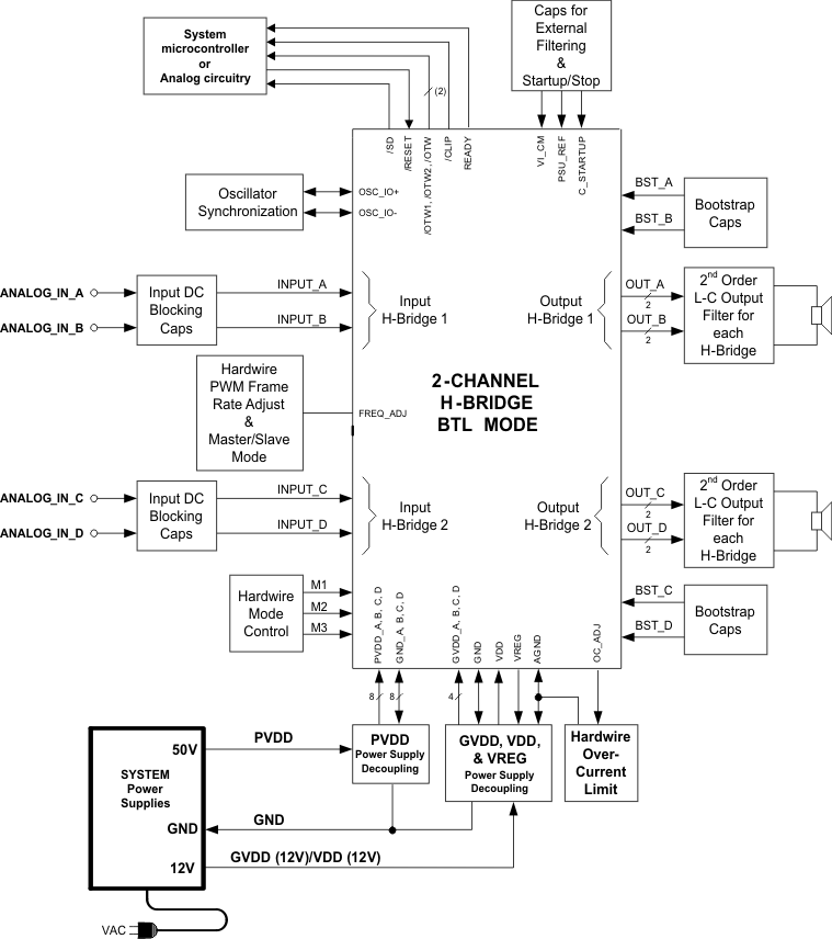 Figure 15. Typical Application Schematic
8.2.1.1 Design Requirements
This device can be configured for BTL, PBTL, or SE mode. Each mode will require a different output configuration.
8.2.1.2 Detailed Design Procedure
- Pin 1 – Overcurrent adjust resistor can be between 24 kΩ to 68 kΩ depending on the application. The lower resistance corresponds to the higher over-current protection level.
- Pin 2 – RESET pin when asserted, it keeps outputs Hi-Z and no PWM switching. This pin can be controlled by a microprocessor.
- Pin 3 – Start-up ramp capacitor should be 4.7 nF for BTL and PBTL configurations, and 10 nF for SE configuration.
- Pins 4, 5, 10, 11 – Differential pair inputs AB and CD. A DC blocking capacitor of 10 µF and an RC of 100 Ω and 100 pF should be placed on each analog input.
- Pin 6 – Analog comparator reference node requires close decoupling capacitor of 1 nF to ground.
- Pin 7, 8, 23, 24, 57, 58 – Ground pins are connected to board ground.
- Pin 9 – Regulator supply filter pin requires 0.1 uF to AGND.
- Pin 12 – Frequency adjust resistor is discussed in Oscillator.
- Pin 13, 14 – Oscillator input/output. When frequency adjust pin is pulled up to VREG, the oscillator pins are configured as inputs.
- Pin 15 – Shutdown pin can be monitored by a microcontroller through GPIO pin. System can decide to assert reset or power down. See Error Reporting.
- Pin 16, 17 – There are two overtemperature warning pins for PHD package. They have two different levels of warning. OTW1 is lower temperature level warning than OTW2. They can be monitored by a microcontroller through GPIO pins. System can decide to turn on fan, lower output power or shutdown. See Error Reporting.
- Pin 18 – Output clip indicator can be monitored by a microcontroller through a GPIO pin. System can decide to lower the volume.
- Pin 19 – Ready pin can be used to signal the system that the device is up and running.
- Pin 20-22 – Mode pins set the input and output configurations. See Table 2 for configuration setting of these pins.
- Pin 25, 26, 55, 56 – Gate drive power pins provide gate voltage for half-bridges. Each needs a 3.3-Ω isolation resistor and a 0.1-uF decoupling capacitor.
- Pins 27, 40, 41, 54 – Bootstrap pins for half-bridges A, B, C, D. Connect 33 nF from this pin to corresponding output pins.
- Pins 28, 29, 36, 37, 44, 45, 53, 54 – Output pins from half-bridges A, B, C, D. Connect appropriate bootstrap capacitors to the output pins. For PWM filtering, each output mode is used with different LC configuration.
- Pins 30, 31, 38, 39, 42, 43, 50, 51 – Power supply pins to half-bridges A, B, C, D. Each PVDD_X has decoupling capacitor connecting to the appropriate GND_X pin.
- Pins 32, 33, 34, 35, 46, 47, 48, 49 – Connect decoupling capacitors of each power input pin to power supply ground pins. Connect these pins to board ground.
- Pins 59-62 – Connect “No connect” pins to board ground. There is no internal connection to these pins.
8.2.1.3 Application Curves
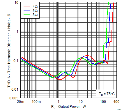 Figure 16. Total Harmonic + Noise vs Output Power
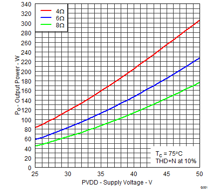 Figure 17. Output Power vs Supply Voltage
8.2.2 Typical Differential-Input BTL Application With BD Modulation Filters
BTL output and differential input configuration is a typical audio class-D (PWM) amplifier. With differential input, the output can be configured for BTL application with BD modulation. The configuration below can also be used with AD modulation. BD modulation gives better channel separation and PSSR performance.
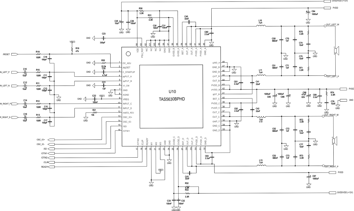 Figure 18. Typical Differential-Input BTL Application With BD Modulation Filters
8.2.3 Typical Differential (2N) PBTL Application With BD Modulation Filters
When there is a need for more power in an audio system, PBTL is a good choice for this application. Paralleling the output after the inductors is recommended. In this configuration, the device can be driven with higher current (lower load impedance). Figure 19 shows the component and pin connections.
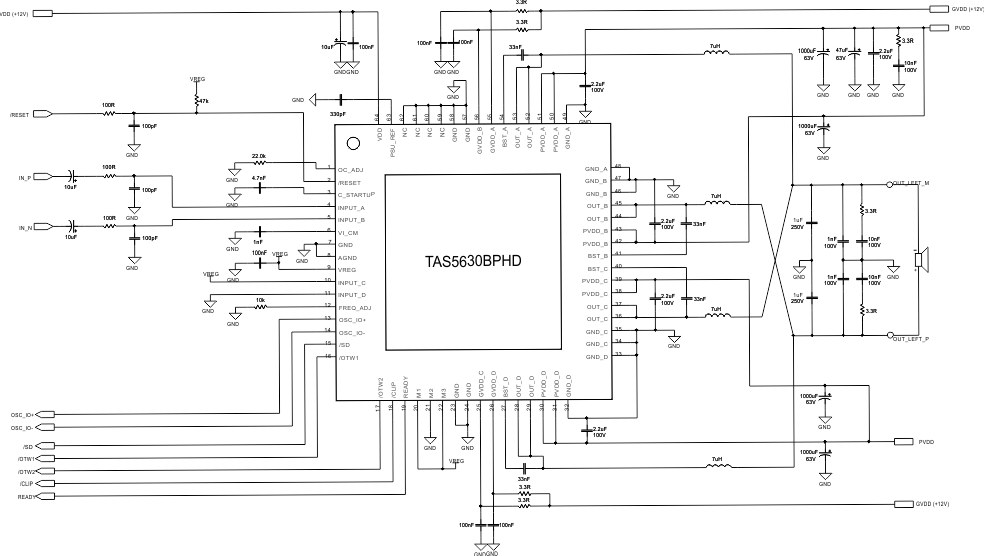 Figure 19. Typical Differential (2N) PBTL Application With BD Modulation Filters
8.2.4 Typical SE Application
Single-ended output configuration is often used for cost effective systems. This device can be configured to drive four independent channels with four different inputs. The delivered power is not as much as BTL configuration. The advantage is that the component count for four channels is the same as two BTL channels. The schematic in this section shows the component and pin connections.
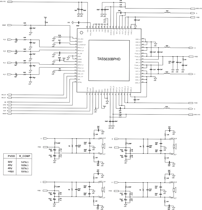 Figure 20. Typical SE Application
8.2.5 Typical 2.1 System Differential-Input BTL and Unbalanced-Input SE Application
One of the attractive features of this device is that it can be configured for mixed BTL and SE outputs. One BTL plus two SE channels make up a 2.1 audio system. While the SE channels are used to drive the front end and right speakers, the BTL channel can deliver higher power and is used to drive a subwoofer. Figure 21 shows the component and pin connections.
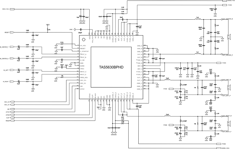 Figure 21. Typical 2.1 System Differential-Input BTL and Unbalanced-Input SE Application
8.2.6 Typical Differential-Input BTL Application With BD Modulation Filters, DKD Package
This is the same application as described in Typical Differential-Input BTL Application With BD Modulation Filters with PHD package. For DKD package an external heatsink is required to dissipate excess heat. In this package, the PCB space is not a limiting factor for dissipating excess heat.
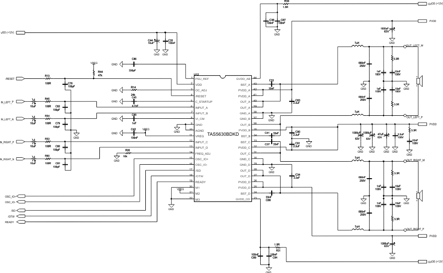 Figure 22. Typical Differential-Input BTL Application With BD Modulation Filters, DKD Package