SLES217D November 2010 – March 2015 TAS5630B
PRODUCTION DATA.
- 1 Features
- 2 Applications
- 3 Description
- 4 Revision History
- 5 Pin Configuration and Functions
- 6 Specifications
-
7 Detailed Description
- 7.1 Overview
- 7.2 Functional Block Diagram
- 7.3
Feature Description
- 7.3.1 Power Supplies
- 7.3.2 System Power-Up and Power-Down Sequence
- 7.3.3 Error Reporting
- 7.3.4 Device Protection System
- 7.3.5 Pin-to-Pin Short-Circuit Protection (PPSC)
- 7.3.6 Overtemperature Protection
- 7.3.7 Undervoltage Protection (UVP) and Power-On Reset (POR)
- 7.3.8 Device Reset
- 7.3.9 Click and Pop in SE-Mode
- 7.3.10 PBTL Overload and Short Circuit
- 7.3.11 Oscillator
- 7.4 Device Functional Modes
-
8 Application and Implementation
- 8.1 Application Information
- 8.2
Typical Application
- 8.2.1 Typical Application Schematic
- 8.2.2 Typical Differential-Input BTL Application With BD Modulation Filters
- 8.2.3 Typical Differential (2N) PBTL Application With BD Modulation Filters
- 8.2.4 Typical SE Application
- 8.2.5 Typical 2.1 System Differential-Input BTL and Unbalanced-Input SE Application
- 8.2.6 Typical Differential-Input BTL Application With BD Modulation Filters, DKD Package
- 9 Power Supply Recommendations
- 10Layout
- 11Device and Documentation Support
- 12Mechanical, Packaging, and Orderable Information
Package Options
Mechanical Data (Package|Pins)
- PHD|64
Thermal pad, mechanical data (Package|Pins)
- PHD|64
Orderable Information
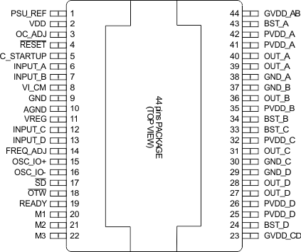
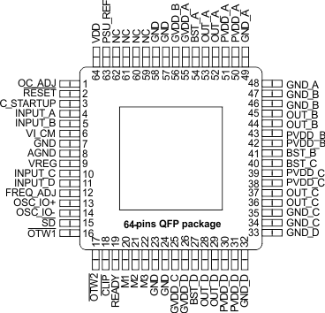
5 Pin Configuration and Functions
DKD Package
44 Pins HSSOP
Top View

PHD Package
64 Pins HTQFP
Top View

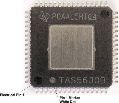
 Figure 1. Pin One Location PHD Package
Pin Functions
| PIN | FUNCTION(1) | DESCRIPTION | ||
|---|---|---|---|---|
| NAME | HTQFP | HSSOP | ||
| AGND | 8 | 10 | P | Analog ground |
| BST_A | 54 | 43 | P | HS bootstrap supply (BST), external 0.033-μF capacitor to OUT_A required. |
| BST_B | 41 | 34 | P | HS bootstrap supply (BST), external 0.033-μF capacitor to OUT_B required. |
| BST_C | 40 | 33 | P | HS bootstrap supply (BST), external 0.033-μF capacitor to OUT_C required. |
| BST_D | 27 | 24 | P | HS bootstrap supply (BST), external 0.033-μF capacitor to OUT_D required. |
| CLIP | 18 | — | O | Clipping warning; open drain; active-low |
| C_STARTUP | 3 | 5 | O | Start-up ramp requires a charging capacitor of 4.7 nF to AGND in BTL mode |
| FREQ_ADJ | 12 | 14 | I | PWM frame-rate-programming pin requires resistor to AGND |
| GND | 7, 23, 24, 57, 58 | 9 | P | Ground |
| GND_A | 48, 49 | 38 | P | Power ground for half-bridge A |
| GND_B | 46, 47 | 37 | P | Power ground for half-bridge B |
| GND_C | 34, 35 | 30 | P | Power ground for half-bridge C |
| GND_D | 32, 33 | 29 | P | Power ground for half-bridge D |
| GVDD_A | 55 | — | P | Gate-drive voltage supply requires 0.1-μF capacitor to GND_A |
| GVDD_B | 56 | — | P | Gate drive voltage supply requires 0.1-μF capacitor to GND_B |
| GVDD_C | 25 | — | P | Gate drive voltage supply requires 0.1-μF capacitor to GND_C |
| GVDD_D | 26 | — | P | Gate drive voltage supply requires 0.1-μF capacitor to GND_D |
| GVDD_AB | — | 44 | P | Gate drive voltage supply requires 0.22-μF capacitor to GND_A/GND_B |
| GVDD_CD | — | 23 | P | Gate drive voltage supply requires 0.22-μF capacitor to GND_C/GND_D |
| INPUT_A | 4 | 6 | I | Input signal for half-bridge A |
| INPUT_B | 5 | 7 | I | Input signal for half-bridge B |
| INPUT_C | 10 | 12 | I | Input signal for half-bridge C |
| INPUT_D | 11 | 13 | I | Input signal for half-bridge D |
| M1 | 20 | 20 | I | Mode selection |
| M2 | 21 | 21 | I | Mode selection |
| M3 | 22 | 22 | I | Mode selection |
| NC | 59–62 | – | — | No connect; pins may be grounded. |
| OC_ADJ | 1 | 3 | O | Analog overcurrent-programming pin requires resistor to AGND. 64-pin package (PHD) = 22 kΩ. 44-pin PSOP3 (DKD) = 24 kΩ |
| OSC_IO+ | 13 | 15 | I/O | Oscillator master/slave output/input |
| OSC_IO– | 14 | 16 | I/O | Oscillator master/slave output/input |
| OTW | — | 18 | O | Overtemperature warning signal, open-drain, active-low |
| OTW1 | 16 | — | O | Overtemperature warning signal, open-drain, active-low |
| OTW2 | 17 | — | O | Overtemperature warning signal, open-drain, active-low |
| OUT_A | 52, 53 | 39, 40 | O | Output, half-bridge A |
| OUT_B | 44, 45 | 36 | O | Output, half-bridge B |
| OUT_C | 36, 37 | 31 | O | Output, half-bridge C |
| OUT_D | 28, 29 | 27, 28 | O | Output, half-bridge D |
| PSU_REF | 63 | 1 | P | PSU reference requires close decoupling of 330 pF to AGND. |
| PVDD_A | 50, 51 | 41, 42 | P | Power-supply input for half-bridge A requires close decoupling of 0.01-μF capacitor in parallel with 2.2-μF capacitor to GND_A. |
| PVDD_B | 42, 43 | 35 | P | Power-supply input for half-bridge B requires close decoupling of 0.01-μF capacitor in parallel with 2.2-μF capacitor to GND_B. |
| PVDD_C | 38, 39 | 32 | P | Power-supply input for half-bridge C requires close decoupling of 0.0- μF capacitor in parallel with 2.2-μF capacitor to GND_C. |
| PVDD_D | 30, 31 | 25, 26 | P | Power-supply input for half-bridge D requires close decoupling of 0.01-μF capacitor in parallel with 2.2-μF capacitor to GND_D. |
| READY | 19 | 19 | O | Normal operation; open-drain; active-high |
| RESET | 2 | 4 | I | Device reset input; active-low |
| SD | 15 | 17 | O | Shutdown signal, open-drain, active-low |
| VDD | 64 | 2 | P | Power supply for digital voltage regulator requires a 10-μF capacitor in parallel with a 0.1-μF capacitor to GND for decoupling. |
| VI_CM | 6 | 8 | O | Analog comparator reference node requires close decoupling of 1 nF to AGND. |
| VREG | 9 | 11 | P | Regulator supply filter pin requires 0.1-μF capacitor to AGND. |
(1) I = Input, O = Output, P = Power