SLOS946A May 2016 – December 2016 TAS5722L
PRODUCTION DATA.
- 1 Features
- 2 Applications
- 3 Description
- 4 Revision History
- 5 Pin Configuration and Functions
- 6 Specifications
-
7 Detailed Description
- 7.1 Overview
- 7.2 Functional Block Diagram
- 7.3 Feature Description
- 7.4 Device Functional Modes
- 7.5
Register Maps
- 7.5.1 I2C Register Map Summary
- 7.5.2
Register Maps
- 7.5.2.1 Device Identification Register (0x00)
- 7.5.2.2 Power Control Register (0x01)
- 7.5.2.3 Digital Control Register 1 (0x02)
- 7.5.2.4 Register Name (offset = ) [reset = ] or (address = ) [reset = ]
- 7.5.2.5 Volume Control Register (0x04)
- 7.5.2.6 Analog Control Register (0x06)
- 7.5.2.7 Fault Configuration and Error Status Register (0x08)
- 7.5.2.8 Digital Clipper 2 Register (0x10)
- 7.5.2.9 Digital Clipper 1 Register (0x11)
- 7.5.2.10 Digital Control Register 3 (0x13)
- 7.5.2.11 Analog Control Register 2 (0x14)
- 8 Applications and Implementation
- 9 Power Supply Recommendations
- 10Layout
- 11Device and Documentation Support
- 12Mechanical, Packaging, and Orderable Information
Package Options
Mechanical Data (Package|Pins)
- RSM|32
Thermal pad, mechanical data (Package|Pins)
- RSM|32
Orderable Information
10 Layout
10.1 Layout Guidelines
- Pay special attention to the power stage power supply layout. Each half bridge has two PVDD input pins so that decoupling capacitors can be placed nearby. Use at least a 0.1-µF capacitor of X5R quality or better for each set of inputs.
- Keep the current circulating loops containing the supply decoupling capacitors, the H-bridges in the device and the connections to the speakers as tight as possible to reduce emissions.
- Use ground planes to provide the lowest impedance for power and signal current between the device and the decoupling capacitors. The area directly under the device should be treated as a central ground area for the device, and all device grounds must be connected directly to that area.
- Use a via pattern to connect the area directly under the device to the ground planes in copper layers below the surface. This connection helps to dissipate heat from the device.
- Avoid interrupting the ground plane with circular traces around the device. Interruption disconnects the copper and interrupt flow of heat and current. Radial copper traces are better to use if necessary.
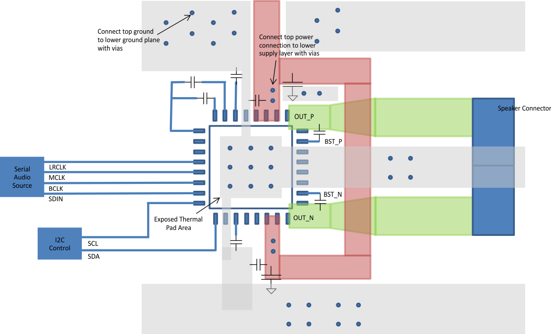
10.2 Layout Example
 Figure 54. Layout Example