SLOS781C July 2013 – November 2017 TAS5760LD
PRODUCTION DATA.
- 1 Features
- 2 Applications
- 3 Description
- 4 Revision History
- 5 Pin Configuration and Functions
-
6 Specifications
- 6.1 Absolute Maximum Ratings
- 6.2 ESD Ratings
- 6.3 Recommended Operating Conditions
- 6.4 Thermal Information
- 6.5 Digital I/O Pins
- 6.6 Master Clock
- 6.7 Serial Audio Port
- 6.8 Protection Circuitry
- 6.9 Speaker Amplifier in All Modes
- 6.10 Speaker Amplifier in Stereo Bridge-Tied Load (BTL) Mode
- 6.11 Speaker Amplifier in Mono Parallel Bridge-Tied Load (PBTL) Mode
- 6.12 Headphone Amplifier and Line Driver
- 6.13 I²C Control Port
- 6.14 Typical Idle, Mute, Shutdown, Operational Power Consumption
- 6.15 Typical Speaker Amplifier Performance Characteristics (Stereo BTL Mode)
- 6.16 Typical Performance Characteristics (Mono PBTL Mode)
- 7 Parameter Measurement Information
-
8 Detailed Description
- 8.1 Overview
- 8.2 Functional Block Diagram
- 8.3 Feature Description
- 8.4
Device Functional Modes
- 8.4.1
Hardware Control Mode
- 8.4.1.1 Speaker Amplifier Shut Down (SPK_SD Pin)
- 8.4.1.2 Serial Audio Port in Hardware Control Mode
- 8.4.1.3 Soft Clipper Control (SFT_CLIP Pin)
- 8.4.1.4 Speaker Amplifier Switching Frequency Select (FREQ/SDA Pin)
- 8.4.1.5 Parallel Bridge Tied Load Mode Select (PBTL/SCL Pin)
- 8.4.1.6 Speaker Amplifier Sleep Enable (SPK_SLEEP/ADR Pin)
- 8.4.1.7 Speaker Amplifier Gain Select (SPK_GAIN [1:0] Pins)
- 8.4.1.8 Considerations for Setting the Speaker Amplifier Gain Structure
- 8.4.2 Software Control Mode
- 8.4.1
Hardware Control Mode
- 8.5
Register Maps
- 8.5.1 Control Port Registers - Quick Reference
- 8.5.2
Control Port Registers - Detailed Description
- 8.5.2.1 Device Identification Register (0x00)
- 8.5.2.2 Power Control Register (0x01)
- 8.5.2.3 Digital Control Register (0x02)
- 8.5.2.4 Volume Control Configuration Register (0x03)
- 8.5.2.5 Left Channel Volume Control Register (0x04)
- 8.5.2.6 Right Channel Volume Control Register (0x05)
- 8.5.2.7 Analog Control Register (0x06)
- 8.5.2.8 Reserved Register (0x07)
- 8.5.2.9 Fault Configuration and Error Status Register (0x08)
- 8.5.2.10 Reserved Controls (9 / 0x09) - (15 / 0x0F)
- 8.5.2.11 Digital Clipper Control 2 Register (0x10)
- 8.5.2.12 Digital Clipper Control 1 Register (0x11)
-
9 Application and Implementation
- 9.1 Application Information
- 9.2
Typical Applications
- 9.2.1
Stereo BTL Using Software Control
- 9.2.1.1 Design Requirements
- 9.2.1.2
Detailed Design Procedure
- 9.2.1.2.1 Startup Procedures- Software Control Mode
- 9.2.1.2.2 Shutdown Procedures- Software Control Mode
- 9.2.1.2.3 Component Selection and Hardware Connections
- 9.2.1.2.4 Recommended Startup and Shutdown Procedures
- 9.2.1.2.5
Headphone and Line Driver Amplifier
- 9.2.1.2.5.1 Charge-Pump Flying Capacitor and DR_VSS Capacitor
- 9.2.1.2.5.2 Decoupling Capacitors
- 9.2.1.2.5.3 Gain-Setting Resistor Ranges
- 9.2.1.2.5.4 Using the Line Driver Amplifier in the TAS5760LD as a Second-Order Filter
- 9.2.1.2.5.5 External Undervoltage Detection
- 9.2.1.2.5.6 Input-Blocking Capacitors
- 9.2.1.2.6 Gain-Setting Resistors
- 9.2.1.3 Application Curves
- 9.2.2 Stereo BTL Using Hardware Control
- 9.2.3 Mono PBTL Using Software Control
- 9.2.4 Mono PBTL Using Hardware Control
- 9.2.1
Stereo BTL Using Software Control
- 10Power Supply Recommendations
- 11Layout
- 12Device and Documentation Support
- 13Mechanical, Packaging, and Orderable Information
Package Options
Mechanical Data (Package|Pins)
- DCA|48
Thermal pad, mechanical data (Package|Pins)
- DCA|48
Orderable Information
6 Specifications
6.1 Absolute Maximum Ratings
over operating free-air temperature range (unless otherwise noted)(1)
(1) Stresses beyond those listed under Absolute Maximum Ratings may cause permanent damage to the device. These are stress ratings only, and functional operation of the device at these or any other conditions beyond those indicated under Recommended Operating Conditions is not implied. Exposure to absolute-maximum-rated conditions for extended periods may affect device reliability.
6.2 ESD Ratings
| VALUE | UNIT | |||
|---|---|---|---|---|
| V(ESD) | Electrostatic discharge | Human body model (HBM), per ANSI/ESDA/JEDEC JS-001(1) | 4000 | V |
| Charged-device model (CDM), per JEDEC specification JESD22-C101(2) | 1500 | |||
(1) JEDEC document JEP155 states that 500-V HBM allows safe manufacturing with a standard ESD control process.
(2) JEDEC document JEP157 states that 250-V CDM allows safe manufacturing with a standard ESD control process.
6.3 Recommended Operating Conditions
over operating free-air temperature range (unless otherwise noted)| MIN | NOM | MAX | UNIT | ||
|---|---|---|---|---|---|
| TA | Ambient Operating Temperature | –25 | 85 | °C | |
| AVDD | AVDD Supply | 4.5 | 16.5 | V | |
| PVDD | PVDD Supply | 4.5 | 16.5 | V | |
| DRVDD, DVDD | DRVDD and DVDD Supply | 2.8 | 3.63 | V | |
| VIH(DR) | Input Logic HIGH for DVDD and DRVDD Referenced Digital Inputs | DVDD | V | ||
| VIL(DR) | Input Logic LOW for DVDD and DRVDD Referenced Digital Inputs | 0 | V | ||
| RHP | Headphone Load | 16 | Ω | ||
| RLD | Line Driver Load | 1 | Ω | ||
| RSPK (BTL) | Minimum Speaker Load in BTL Mode | 4 | Ω | ||
| RSPK (PBTL) | Minimum Speaker Load in PBTL Mode | 2 | Ω | ||
6.4 Thermal Information
| THERMAL METRIC(1) | TAS5760LD | UNIT | ||
|---|---|---|---|---|
| DCA [HTSSOP] | DCA [HTSSOP] | |||
| 48 PIN(2) | 48 PIN(3) | |||
| θJA | Junction-to-ambient thermal resistance | 60.3 | 30.2 | °C/W |
| θJC(top) | Junction-to-case (top) thermal resistance | 16 | 14.3 | °C/W |
| θJB | Junction-to-board thermal resistance | 12 | 12.7 | °C/W |
| ψJT | Junction-to-top characterization parameter | 0.4 | 0.6 | °C/W |
| ψJB | Junction-to-board characterization parameter | 11.9 | 12.7 | °C/W |
| θJC(bottom) | Junction-to-case (bottom) thermal resistance | 0.8 | 0.7 | °C/W |
(1) For more information about traditional and new thermal metrics, see the Semiconductor and IC Package Thermal Metrics application report.
(2) JEDEC Standard 2 Layer Board
(3) JEDEC Standard 4 Layer Board
6.5 Digital I/O Pins
over operating free-air temperature range (unless otherwise noted)6.6 Master Clock
over operating free-air temperature range (unless otherwise noted)6.7 Serial Audio Port
over operating free-air temperature range (unless otherwise noted)| PARAMETER | TEST CONDITIONS | MIN | TYP | MAX | UNIT | |
|---|---|---|---|---|---|---|
| DSCLK | Allowable SCLK Duty Cycle | 45% | 50% | 55% | ||
| tH_L | Time high and low, SCLK, LRCK, SDIN | 10 | ns | |||
| tSU
tHLD |
Setup and Hold time. LRCK, SDIN input to SCLK edge | Input tRISE ≤ 1 ns, input tFALL ≤ 1 ns | 5 | ns | ||
| Input tRISE ≤ 4 ns, input tFALL ≤ 4 ns | 8 | |||||
| Input tRISE ≤ 8 ns, input tFALL ≤ 8 ns | 12 | |||||
| tRISE | Rise-time SCLK, LRCK, SDIN inputs | 8 | ns | |||
| tFALL | Fall-time SCLK, LRCK, SDIN inputs | 8 | ns | |||
| fS | Supported Input Sample Rates | Sample rates above 48kHz supported by "double speed mode," which is activated through the I²C control port | 32 | 96 | kHz | |
| fSCLK | Supported SCLK Frequencies | Values include: 32, 48, 64 | 32 | 64 | fS | |
6.8 Protection Circuitry
over operating free-air temperature range (unless otherwise noted)| PARAMETER | TEST CONDITIONS | MIN | TYP | MAX | UNIT | |
|---|---|---|---|---|---|---|
| OVERTHRES(PVDD) | PVDD Overvoltage Error Threshold | PVDD Rising | 18 | V | ||
| OVEFTHRES(PVDD) | PVDD Overvoltage Error Threshold | PVDD Falling | 17.3 | V | ||
| UVEFTHRES(PVDD) | PVDD Undervoltage Error (UVE) Threshold | PVDD Falling | 3.95 | V | ||
| UVERTHRES(PVDD) | PVDD UVE Threshold (PVDD Rising) | PVDD Rising | 4.15 | V | ||
| OTETHRES | Overtemperature Error (OTE) Threshold | 150 | °C | |||
| OTEHYST | Overtemperature Error (OTE) Hysteresis | 15 | °C | |||
| OCETHRES | Overcurrent Error (OCE) Threshold for each BTL Output | PVDD= 15V, TA = 25 °C | 7 | A | ||
| DCETHRES | DC Error (DCE) Threshold | PVDD= 12V, TA = 25 °C | 2.6 | V | ||
| TSPK_FAULT | Speaker Amplifier Fault Time Out period | DC Detect Error | 650 | ms | ||
| OTE or OCP Fault | 1.3 | s | ||||
| UVETHRES(DRVDD) | Undervoltage Error (UVE) Threshold for headphone and line driver amplifier | Sensed on DR_UVE pin | 1.25 | V | ||
| ILIMIT(DR) | Current Sourcing Limit of the Headphone and line driver amplifier | 68 | mA | |||
6.9 Speaker Amplifier in All Modes
over operating free-air temperature range (unless otherwise noted)| PARAMETER | TEST CONDITIONS | MIN | TYP | MAX | UNIT | |
|---|---|---|---|---|---|---|
| AV00 | Speaker Amplifier Gain with SPK_GAIN[1:0] Pins = 00 | Hardware Control Mode (Additional gain settings available in Software Control Mode)(1) | 25.2 | dBV | ||
| AV01 | Speaker Amplifier Gain with SPK_GAIN[1:0] Pins = 01 | Hardware Control Mode (Additional gain settings available in Software Control Mode)(1) | 28.6 | dBV | ||
| AV10 | Speaker Amplifier Gain with SPK_GAIN[1:0] Pins = 10 | Hardware Control Mode (Additional gain settings available in Software Control Mode)(1) | 31 | dBV | ||
| AV11 | Speaker Amplifier Gain with SPK_GAIN[1:0] Pins = 11 | (This setting places the device in Software Control Mode) | (Set via I²C) | |||
| |VOS|(SPK_AMP) | Speaker Amplifier DC Offset | BTL, Worst case over voltage, gain settings | 10 | mV | ||
| PBTL, Worst case over voltage, gain settings | 15 | mV | ||||
| fSPK_AMP(0) | Speaker Amplifier Switching Frequency when PWM_FREQ Pin = 0 | (Hardware Control Mode. Additional switching rates available in Software Control Mode.) | 16 | fS | ||
| fSPK_AMP(1) | Speaker Amplifier Switching Frequency when PWM_FREQ Pin = 1 | (Hardware Control Mode. Additional switching rates available in Software Control Mode.) | 8 | fS | ||
| RDS(ON) | On Resistance of Output MOSFET (both high-side and low-side) | PVDD = 15 V, TA = 25 °C, Die Only | 120 | mΩ | ||
| PVDD= 15V, TA = 25 °C, Includes: Die, Bond Wires, Leadframe | 150 | mΩ | ||||
| fC | –3-dB Corner Frequency of High-Pass Filter | fS = 44.1 kHz | 3.7 | Hz | ||
| fS = 48 kHz | 4 | |||||
| fS = 88.2 kHz | 7.4 | |||||
| fS = 96 kHz | 8 | |||||
(1) The digital boost block contributes +6dB of gain to this value. The audio signal must be kept below -6dB to avoid clipping the digital audio path.
6.10 Speaker Amplifier in Stereo Bridge-Tied Load (BTL) Mode
input signal is 1 kHz Sine, specifications are over operating free-air temperature range (unless otherwise noted)| PARAMETER | TEST CONDITIONS | MIN | TYP | MAX | UNIT | |
|---|---|---|---|---|---|---|
| ICN(SPK) | Idle Channel Noise | PVDD = 12 V, SPK_GAIN[1:0] Pins = 00, RSPK = 8Ω, A-Weighted |
- | 66 | - | µVrms |
| PVDD = 15 V, SPK_GAIN[1:0] Pins = 01, RSPK = 8Ω, A-Weighted |
- | 75 | - | µVrms | ||
| PO(SPK) | Maximum Instantaneous Output Power Per. Ch. | PVDD = 12 V, SPK_GAIN[1:0] Pins = 00, RSPK = 4Ω, THD+N = 0.1%, |
- | 14.2 | - | W |
| PVDD = 12 V, SPK_GAIN[1:0] Pins = 00, RSPK = 8Ω, THD+N = 0.1% |
- | 8 | - | W | ||
| PVDD = 15 V, SPK_GAIN[1:0] Pins = 01, RSPK = 4Ω, THD+N = 0.1%, |
- | 21.9 | - | W | ||
| PVDD = 15 V, SPK_GAIN[1:0] Pins = 01, RSPK = 8Ω, THD+N = 0.1% |
- | 12.5 | - | W | ||
| PO(SPK) | Maximum Continuous Output Power Per. Ch.(1) | PVDD = 12 V, SPK_GAIN[1:0] Pins = 00, RSPK = 4Ω, THD+N = 0.1%, |
- | 14 | - | W |
| PVDD = 12 V, SPK_GAIN[1:0] Pins = 00, RSPK = 8Ω, THD+N = 0.1% |
- | 8 | - | W | ||
| PVDD = 15 V, SPK_GAIN[1:0] Pins = 01, RSPK = 4Ω, THD+N = 0.1%, |
- | 13.25 | - | W | ||
| PVDD = 15 V, SPK_GAIN[1:0] Pins = 01, RSPK = 8Ω, THD+N = 0.1% |
- | 12.5 | - | W | ||
| SNR(SPK) | Signal to Noise Ratio (Referenced to THD+N = 1%) | PVDD = 12 V, SPK_GAIN[1:0] Pins = 00, RSPK = 8Ω, A-Weighted, -60dBFS Input |
- | 99.7 | - | dB |
| PVDD = 15 V, SPK_GAIN[1:0] Pins = 01, RSPK = 8Ω, A-Weighted, -60dBFS Input |
- | 98.2 | - | dB | ||
| THD+N(SPK) | Total Harmonic Distortion and Noise | PVDD = 12 V, SPK_GAIN[1:0] Pins = 00, RSPK = 4Ω, Po = 1 W |
- | 0.02% | - | |
| PVDD = 12 V, SPK_GAIN[1:0] Pins = 00, RSPK = 8Ω, Po = 1 W |
- | 0.03% | - | |||
| PVDD = 15 V, SPK_GAIN[1:0] Pins = 01, RSPK = 4Ω, Po = 1 W |
- | 0.03% | - | |||
| PVDD = 15 V, SPK_GAIN[1:0] Pins = 01, RSPK = 8Ω, Po = 1 W |
- | 0.03% | - | |||
| X-Talk(SPK) | Cross-talk (worst case between LtoR and RtoL coupling) | PVDD = 12 V, SPK_GAIN[1:0] Pins = 00, RSPK = 8Ω, Input Signal 250 mVrms, 1kHz Sine |
- | -92 | - | dB |
| PVDD = 15 V, SPK_GAIN[1:0] Pins = 01, RSPK = 8Ω, Input Signal 250 mVrms, 1kHz Sine |
- | -93 | - | dB | ||
(1) The continuous power output of any amplifier is determined by the thermal performance of the amplifier as well as limitations placed on it by the system around it, such as the PCB configuration and the ambient operating temperature. The performance characteristics listed in this section are achievable on the TAS5760LD's EVM, which is representative of the poplular "2 Layers / 1oz Copper" PCB configuration in a size that is representative of the amount of area often provided to the amplifier section of popular consumer audio electronics. As can be seen in the instantaneous power portion of this table, more power can be delivered from the TAS5760LD if steps are taken to pull more heat out of the device. For instance, using a board with more layers or adding a small heatsink will result in an increase of continuous power, up to and including the instantaneous power level. This behavior can also been seen in the POUT vs. PVDD plots shown in the typical performance plots section of this data sheet.
6.11 Speaker Amplifier in Mono Parallel Bridge-Tied Load (PBTL) Mode
input signal is 1 kHz Sine, specifications are over operating free-air temperature range (unless otherwise noted)| PARAMETER | TEST CONDITIONS | MIN | TYP | MAX | UNIT | |
|---|---|---|---|---|---|---|
| ICN | Idle Channel Noise | PVDD = 12 V, SPK_GAIN[1:0] Pins = 00, RSPK = 8Ω, A-Weighted |
- | 69 | - | µVrms |
| PVDD = 15 V, SPK_GAIN[1:0] Pins = 01, RSPK = 8Ω, A-Weighted |
- | 85 | - | µVrms | ||
| PO(SPK) | Maximum Instantaneous Output Power | PVDD = 12 V, SPK_GAIN[1:0] Pins = 00, RSPK = 2Ω, THD+N = 0.1%, |
- | 28.6 | - | W |
| PVDD = 12 V, SPK_GAIN[1:0] Pins = 00, RSPK = 4Ω, THD+N = 0.1%, |
- | 15.9 | - | W | ||
| PVDD = 12 V, SPK_GAIN[1:0] Pins = 00, RSPK = 8Ω, THD+N = 0.1% |
- | 8.4 | - | W | ||
| PVDD = 15 V, SPK_GAIN[1:0] Pins = 01, RSPK = 2Ω, THD+N = 0.1%, |
- | 43.2 | - | W | ||
| PVDD = 15 V, SPK_GAIN[1:0] Pins = 01, RSPK = 4Ω, THD+N = 0.1%, |
- | 25 | - | W | ||
| PVDD = 15 V, SPK_GAIN[1:0] Pins = 01, RSPK = 8Ω, THD+N = 0.1% |
- | 13.3 | - | W | ||
| PO(SPK) | Maximum Continuous Output Power(1) | PVDD = 12 V, SPK_GAIN[1:0] Pins = 00, RSPK = 2Ω, THD+N = 0.1%, |
- | 30 | - | W |
| PVDD = 12 V, SPK_GAIN[1:0] Pins = 00, RSPK = 4Ω, THD+N = 0.1%, |
- | 15.9 | - | W | ||
| PVDD = 12 V, SPK_GAIN[1:0] Pins = 00, RSPK = 8Ω, THD+N = 0.1% |
- | 8.4 | - | W | ||
| PVDD = 15 V, SPK_GAIN[1:0] Pins = 01, RSPK = 2Ω, THD+N = 0.1%, |
- | 28.5 | - | W | ||
| PVDD = 15 V, SPK_GAIN[1:0] Pins = 01, RSPK = 4Ω, THD+N = 0.1%, |
- | 25 | - | W | ||
| PVDD = 15 V, SPK_GAIN[1:0] Pins = 01, RSPK = 8Ω, THD+N = 0.1% |
- | 13.3 | - | W | ||
| SNR | Signal to Noise Ratio (Referenced to THD+N = 1%) | PVDD = 12 V, SPK_GAIN[1:0] Pins = 00, RSPK = 8Ω, A-Weighted, -60dBFS Input |
- | 100.4 | - | dB |
| PVDD = 15 V, SPK_GAIN[1:0] Pins = 01, RSPK = 8Ω, A-Weighted, -60dBFS Input |
- | 99.5 | - | dB | ||
| THD+N(SPK) | Total Harmonic Distortion and Noise | PVDD = 12 V, SPK_GAIN[1:0] Pins = 00, RSPK = 2Ω, Po = 1 W |
- | 0.03% | - | |
| PVDD = 12 V, SPK_GAIN[1:0] Pins = 00, RSPK = 4Ω, Po = 1 W |
- | 0.02% | - | |||
| PVDD = 12 V, SPK_GAIN[1:0] Pins = 00, RSPK = 8Ω, Po = 1 W |
- | 0.02% | - | |||
| PVDD = 15 V, SPK_GAIN[1:0] Pins = 01, RSPK = 2Ω, Po = 1 W |
- | 0.03% | - | |||
| PVDD = 15 V, SPK_GAIN[1:0] Pins = 01, RSPK = 4Ω, Po = 1 W |
- | 0.02% | - | |||
| PVDD = 15 V, SPK_GAIN[1:0] Pins = 01, RSPK = 8Ω, Po = 1 W |
- | 0.02% | - | |||
(1) The continuous power output of any amplifier is determined by the thermal performance of the amplifier as well as limitations placed on it by the system around it, such as the PCB configuration and the ambient operating temperature. The performance characteristics listed in this section are achievable on the TAS5760LD's EVM, which is representative of the poplular "2 Layers / 1oz Copper" PCB configuration in a size that is representative of the amount of area often provided to the amplifier section of popular consumer audio electronics. As can be seen in the instantaneous power portion of this table, more power can be delivered from the TAS5760LD if steps are taken to pull more heat out of the device. For instance, using a board with more layers or adding a small heatsink will result in an increase of continuous power, up to and including the instantaneous power level. This behavior can also been seen in the POUT vs. PVDD plots shown in the typical performance plots section of this data sheet.
6.12 Headphone Amplifier and Line Driver
input signal is 1 kHz Sine, specifications are over operating free-air temperature range (unless otherwise noted)| PARAMETER | TEST CONDITIONS | MIN | TYP | MAX | UNIT | |
|---|---|---|---|---|---|---|
| Input to Output Attenuation when muted | 80 | dB | ||||
| |VOS|(DR) | Output Offset Voltage of Headphone Amplifier and Line Driver | 0.5 | mV | |||
| fCP | Charge Pump Switching Frequency | 200 | 300 | 400 | kHz | |
| ICN(HP) | Idle Channel Noise | R(HP) = 32 Ω, A-Weighted | 13 | µVrms | ||
| ICN(LD) | Idle Channel Noise | R(LD) = 3 kΩ, A-Weighted | 11 | µVrms | ||
| Po(HP) | Headphone Amplifier Output Power | R(HP) = 16 Ω, THD+N = 1%, Outputs in Phase | 40 | mW | ||
| PSRR(DR) | Power Supply Rejection Ratio of Headphone Amplifier and Line Driver | 80 | dB | |||
| SNR(HP) | Signal to Noise Ratio | (Referenced to 25 mW Output Signal), R(HP) = 16 Ω, A-Weighted | 96 | dB | ||
| SNR(LD) | Signal to Noise Ratio | (Referenced to 2 Vrms Output Signal), R(LD) = 3 kΩ, A-Weighted | 90 | 105 | dB | |
| THD+N(HP) | Total Harmonic Distortion and Noise for the Headphone Amplifier | PO(HP) = 10 mW | 0.01% | |||
| THD+N(LD) | Total Harmonic Distortion and Noise for the Line Driver | VO(LD) = 2 Vrms | 0.002% | |||
| Vo(LD) | Line Driver Output Voltage | THD+N = 1%, R(LD) = 3kΩ, Outputs in Phase | 2 | 2.4 | Vrms | |
| X-Talk(HP) | Cross-talk (worst case between LtoR and RtoL coupling) | PO(HP) = 20 mW | –90 | dB | ||
| X-Talk(LD) | Cross-talk (worst case between LtoR and RtoL coupling) | Vo = 1 Vrms | –111 | dB | ||
| ZO(DR) | Output Impedance when muted | DR_MUTE = LOW | 110 | mΩ | ||
| IMUTE(DR) | Current drawn from DRVDD supply in mute | DR_MUTE = LOW | 12 | mA | ||
| IDRVDD(HP) | Current drawn from DRVDD supply with headphone | DR_MUTE = HIGH, PO(HP) = 25 mW, Input = 1kHz | 60 | mA | ||
| IDRVDD(LD) | Current drawn from DRVDD supply with line driver | DR_MUTE = HIGH, VO(LD) = 2 Vrms, Input = 1kHz | 12 | mA | ||
6.13 I²C Control Port
specifications are over operating free-air temperature range (unless otherwise noted)| PARAMETER | TEST CONDITIONS | MIN | TYP | MAX | UNIT | |
|---|---|---|---|---|---|---|
| CL(I²C) | Allowable Load Capacitance for Each I²C Line | 400 | pF | |||
| fSCL | Support SCL frequency | No Wait States | 400 | kHz | ||
| tbuf | Bus Free time between STOP and START conditions | 1.3 | µS | |||
| tf(I²C) | Rise Time, SCL and SDA | 300 | ns | |||
| th1(I²C) | Hold Time, SCL to SDA | 0 | ns | |||
| th2(I²C) | Hold Time, START condition to SCL | 0.6 | µs | |||
| tI²C(start) | I²C Startup Time | 12 | mS | |||
| tr(I²C) | Rise Time, SCL and SDA | 300 | ns | |||
| tsu1(I²C) | Setup Time, SDA to SCL | 100 | ns | |||
| tsu2(I²C) | Setup Time, SCL to START condition | 0.6 | µS | |||
| tsu3(I²C) | Setup Time, SCL to STOP condition | 0.6 | µS | |||
| Tw(H) | Required Pulse Duration, SCL HIGH | 0.6 | µS | |||
| Tw(L) | Required Pulse Duration, SCL LOW | 1.3 | µS | |||
6.14 Typical Idle, Mute, Shutdown, Operational Power Consumption
input signal is 1 kHz Sine, specifications are over operating free-air temperature range (unless otherwise noted)| VPVDD
[V] |
RSPK
[Ω] |
SPEAKER AMPLIFIER STATE | IPVDD+AVDD
[mA] |
IDVDD
[mA] |
PDISS
[W] |
|
|---|---|---|---|---|---|---|
| 6 | 4 | fSPK_AMP = 384kHz | Idle | 23.48 | 3.73 | 0.15 |
| 8 | 23.44 | 3.72 | 0.15 | |||
| 4 | Mute | 23.53 | 3.72 | 0.15 | ||
| 8 | 23.46 | 3.72 | 0.15 | |||
| 4 | Sleep | 13.26 | 0.48 | 0.08 | ||
| 8 | 13.27 | 0.53 | 0.08 | |||
| 4 | Shutdown | 0.046 | 0.04 | 0 | ||
| 8 | 0.046 | 0.03 | 0 | |||
| 4 | fSPK_AMP = 768kHz | Idle | 30.94 | 3.71 | 0.2 | |
| 8 | 30.94 | 3.71 | 0.2 | |||
| 4 | Mute | 29.37 | 3.71 | 0.19 | ||
| 8 | 29.39 | 3.71 | 0.19 | |||
| 4 | Sleep | 13.24 | 0.5 | 0.08 | ||
| 8 | 13.23 | 0.52 | 0.08 | |||
| 4 | Shutdown | 0.046 | 0.03 | 0 | ||
| 8 | 0.046 | 0.03 | 0 | |||
| 4 | fSPK_AMP = 1152kHz | Idle | 39.39 | 3.7 | 0.25 | |
| 8 | 39.43 | 3.7 | 0.25 | |||
| 4 | Mute | 36.91 | 3.7 | 0.23 | ||
| 8 | 36.9 | 3.69 | 0.23 | |||
| 4 | Sleep | 13.17 | 0.53 | 0.08 | ||
| 8 | 13.13 | 0.45 | 0.08 | |||
| 4 | Shutdown | 0.046 | 0.03 | 0 | ||
| 8 | 0.046 | 0.03 | 0 | |||
| 12 | 4 | fSPK_AMP = 384kHz | Idle | 32.95 | 3.74 | 0.41 |
| 8 | 32.93 | 3.73 | 0.41 | |||
| 4 | Mute | 32.98 | 3.73 | 0.41 | ||
| 8 | 32.97 | 3.73 | 0.41 | |||
| 4 | Sleep | 12.71 | 0.47 | 0.15 | ||
| 8 | 12.75 | 0.5 | 0.15 | |||
| 4 | Shutdown | 0.053 | 0.04 | 0 | ||
| 8 | 0.053 | 0.04 | 0 | |||
| 4 | fSPK_AMP = 768kHz | Idle | 44.84 | 3.73 | 0.55 | |
| 8 | 44.82 | 3.73 | 0.55 | |||
| 4 | Mute | 42.71 | 3.72 | 0.52 | ||
| 8 | 42.66 | 3.72 | 0.52 | |||
| 4 | Sleep | 12.71 | 0.49 | 0.15 | ||
| 8 | 12.73 | 0.52 | 0.15 | |||
| 4 | Shutdown | 0.063 | 0.03 | 0 | ||
| 8 | 0.053 | 0.03 | 0 | |||
| 4 | fSPK_AMP = 1152kHz | Idle | 59.3 | 3.73 | 0.72 | |
| 8 | 59.3 | 3.73 | 0.72 | |||
| 4 | Mute | 55.74 | 3.72 | 0.68 | ||
| 8 | 55.74 | 3.72 | 0.68 | |||
| 4 | Sleep | 12.67 | 0.49 | 0.15 | ||
| 8 | 12.61 | 0.43 | 0.15 | |||
| 4 | Shutdown | 0.053 | 0.02 | 0 | ||
| 8 | 0.053 | 0.03 | 0 | |||
6.15 Typical Speaker Amplifier Performance Characteristics (Stereo BTL Mode)
At TA = 25°C, fSPK_AMP = 384 kHz, input signal is 1 kHz Sine, unless otherwise noted. Filter used for 8 Ω = 22 µH + 0.68 µF, Filter used for 6 Ω = 15 µH + 0.68 µF, Filter used for 4 Ω = 10 µH + 0.68 µF unless otherwise noted.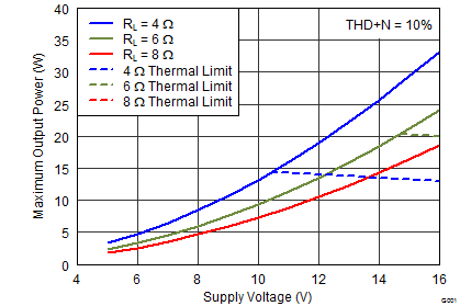
Thermal Limits are referenced to TAS5760xxEVM Rev D
Figure 1. Output Power vs PVDD
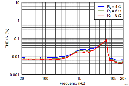
PVDD = 12 V, POSPK = 1 W
Figure 3. THD+N vs Frequency
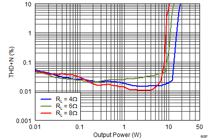
PVDD = 12 V, Both Channels Driven
Figure 5. THD+N vs Output Power
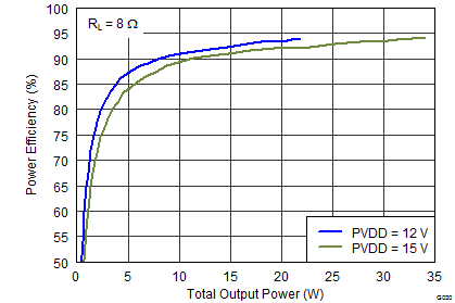 Figure 7. Efficiency vs Output Power
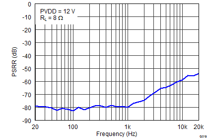 Figure 9. PVDD PSRR vs Frequency
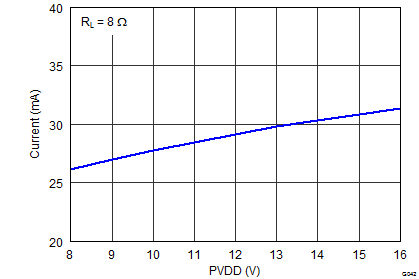 Figure 11. Idle Current Draw vs PVDD (Filterless)
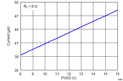 Figure 13. Shutdown Current Draw vs PVDD (Filterless)
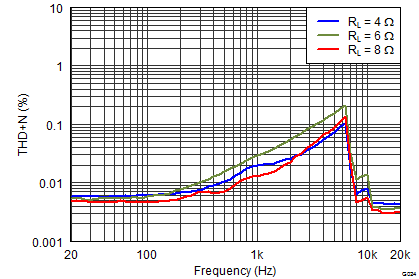
PVDD = 12 V, POSPK = 1 W
Figure 2. THD+N vs Frequency
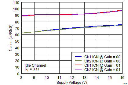 Figure 4. Idle Channel Noise vs PVDD
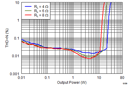
PVDD = 12 V, Both Channels Driven
Figure 6. THD+N vs Output Power
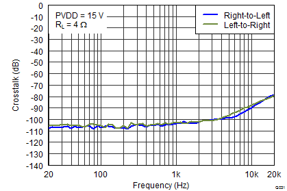 Figure 8. Crosstalk vs Frequency
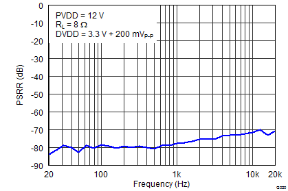 Figure 10. DVDD PSRR vs Frequency
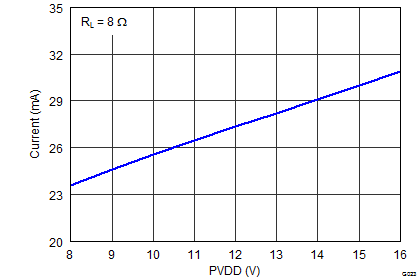
With LC Filter as shown on the EVM
Figure 12. Idle Current Draw vs PVDD
Filter used for 8 Ω = 22 µH + 0.68 µF, Filter used for 6 Ω = 15 µH + 0.68 µF, Filter used for 4 Ω = 10 µH + 0.68 µF unless otherwise noted.
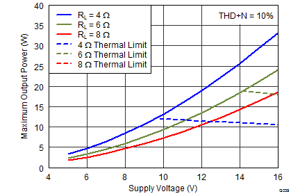
Thermal Limits are referenced to TAS5760xxEVM Rev D
Figure 14. Output Power vs PVDD
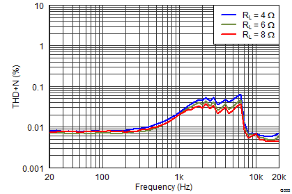
PVDD = 12 V, POSPK = 1 W
Figure 16. THD+N vs Frequency
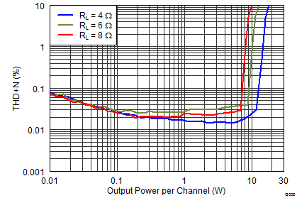
PVDD = 12 V, Both Channels Driven
Figure 18. THD+N vs Output Power
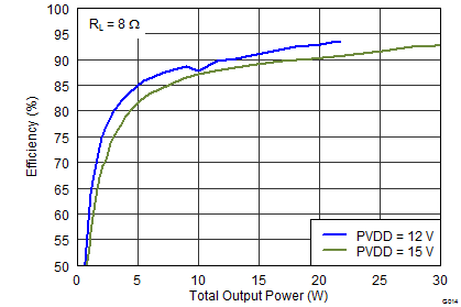 Figure 20. Efficiency vs Output Power
 Figure 22. PVDD PSRR vs Frequency
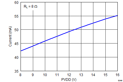 Figure 24. Idle Current Draw vs PVDD (with LC Filter as shown on EVM)
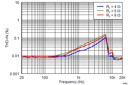
PVDD = 12 V, POSPK = 1 W
Figure 15. THD+N vs Frequency
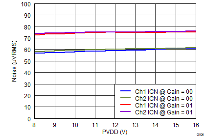 Figure 17. Idle Channel Noise vs PVDD
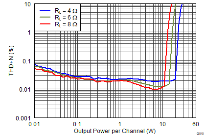
PVDD = 12 V, Both Channels Driven
Figure 19. THD+N vs Output Power
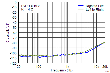 Figure 21. Crosstalk vs Frequency
 Figure 23. Idle Current Draw vs PVDD (Filterless)
 Figure 25. Shutdown Current Draw vs PVDD (Filterless)
6.16 Typical Performance Characteristics (Mono PBTL Mode)
At TA = 25°C, fSPK_AMP = 384 kHz, input signal is 1 kHz Sine unless otherwise noted.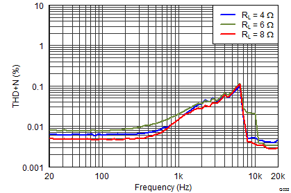
PVDD = 12 V, POSPK = 1 W
Figure 26. THD+N vs Frequency
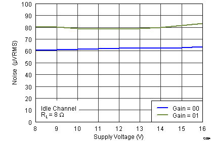 Figure 28. Idle Channel Noise vs PVDD
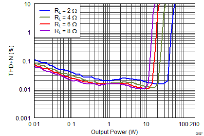
PVDD = 12 V with 1 kHz Sine Input
Figure 30. THD+N vs Output Power
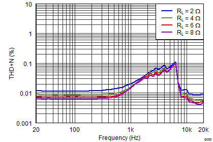
PVDD = 12 V, POSPK = 1 W
Figure 27. THD+N vs Frequency
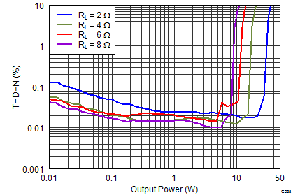
PVDD = 12 V with 1 kHz Sine Input
Figure 29. THD+N vs Output Power
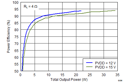 Figure 31. Efficiency vs Output Power
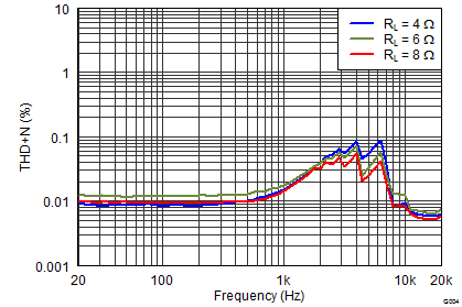
PVDD = 12 V, POSPK = 1 W
Figure 32. THD+N vs Frequency
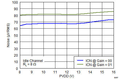 Figure 34. Idle Channel Noise vs PVDD
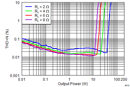 Figure 36. THD+N vs Output Power with PVDD = 12 V
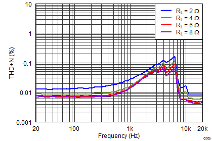
PVDD = 12 V, POSPK = 1 W
Figure 33. THD+N vs Frequency
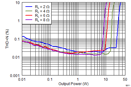 Figure 35. THD+N vs Output Power with PVDD = 12 V
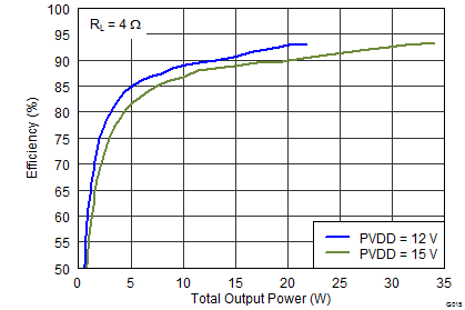 Figure 37. Efficiency vs Output Power