-
TAS5780M Digital Input, Closed-Loop Class-D Amplifier with 96-kHz Processing
- 1 Features
- 2 Applications
- 3 Description
- 4 Revision History
- 5 Device Comparison Table
- 6 Pin Configuration and Functions
-
7 Specifications
- 7.1 Absolute Maximum Ratings
- 7.2 ESD Ratings
- 7.3 Recommended Operating Conditions
- 7.4 Thermal Information
- 7.5 Electrical Characteristics
- 7.6 Power Dissipation Characteristics
- 7.7 MCLK Timing
- 7.8 Serial Audio Port Timing - Slave Mode
- 7.9 Serial Audio Port Timing - Master Mode
- 7.10 I2C Bus Timing - Standard
- 7.11 I2C Bus Timing - Fast
- 7.12 SPK_MUTE Timing
- 7.13 Typical Characteristics
- 8 Parametric Measurement Information
-
9 Detailed Description
- 9.1 Overview
- 9.2 Functional Block Diagram
- 9.3
Feature Description
- 9.3.1 Power-on-Reset (POR) Function
- 9.3.2 Device Clocking
- 9.3.3
Serial Audio Port
- 9.3.3.1 Clock Master Mode from Audio Rate Master Clock
- 9.3.3.2 Clock Master from a Non-Audio Rate Master Clock
- 9.3.3.3 Clock Slave Mode with 4-Wire Operation (SCLK, MCLK, LRCK/FS, SDIN)
- 9.3.3.4 Clock Slave Mode with SCLK PLL to Generate Internal Clocks (3-Wire PCM)
- 9.3.3.5 Serial Audio Port - Data Formats and Bit Depths
- 9.3.3.6 Input Signal Sensing (Power-Save Mode)
- 9.3.4 Enable Device
- 9.3.5 Volume Control
- 9.3.6 Adjustable Amplifier Gain and Switching Frequency Selection
- 9.3.7
Error Handling and Protection Suite
- 9.3.7.1 Device Overtemperature Protection
- 9.3.7.2 SPK_OUTxx Overcurrent Protection
- 9.3.7.3 Internal VAVDD Undervoltage-Error Protection
- 9.3.7.4 Internal VPVDD Undervoltage-Error Protection
- 9.3.7.5 Internal VPVDD Overvoltage-Error Protection
- 9.3.7.6 External Undervoltage-Error Protection
- 9.3.7.7 Internal Clock Error Notification (CLKE)
- 9.3.8 GPIO Port and Hardware Control Pins
- 9.3.9 I2C Communication Port
- 9.4 Device Functional Modes
- 9.5
Programming
- 9.5.1 Audio Processing Features
- 9.5.2 Processing Block Description
- 9.5.3 Other Processing Block Features
- 9.5.4 Checksum
- 10Application and Implementation
- 11Power Supply Recommendations
- 12Layout
-
13Register Maps
- 13.1
Registers - Page 0
- 13.1.1 Register 1 (0x01)
- 13.1.2 Register 2 (0x02)
- 13.1.3 Register 3 (0x03)
- 13.1.4 Register 4 (0x04)
- 13.1.5 Register 5 (0x05)
- 13.1.6 Register 6 (0x06)
- 13.1.7 Register 7 (0x07)
- 13.1.8 Register 8 (0x08)
- 13.1.9 Register 9 (0x09)
- 13.1.10 Register 10 (0x0A)
- 13.1.11 Register 12 (0x0C)
- 13.1.12 Register 13 (0x0D)
- 13.1.13 Register 14 (0x0E)
- 13.1.14 Register 15 (0x0F)
- 13.1.15 Register 16 (0x10)
- 13.1.16 Register 17 (0x11)
- 13.1.17 Register 18 (0x12)
- 13.1.18 Register 19 (0x13)
- 13.1.19 Register 20 (0x14)
- 13.1.20 Register 21 (0x15)
- 13.1.21 Register 22 (0x16)
- 13.1.22 Register 23 (0x17)
- 13.1.23 Register 24 (0x18)
- 13.1.24 Register 25 (0x19)
- 13.1.25 Register 26 (0x1A)
- 13.1.26 Register 27 (0x1B)
- 13.1.27 Register 28 (0x1C)
- 13.1.28 Register 29 (0x1D)
- 13.1.29 Register 30 (0x1E)
- 13.1.30 Register 31 (0x1F)
- 13.1.31 Register 32 (0x20)
- 13.1.32 Register 33 (0x21)
- 13.1.33 Register 34 (0x22)
- 13.1.34 Register 35 (0x23)
- 13.1.35 Register 37 (0x25)
- 13.1.36 Register 38 (0x26)
- 13.1.37 Register 39 (0x27)
- 13.1.38 Register 40 (0x28)
- 13.1.39 Register 41 (0x29)
- 13.1.40 Register 42 (0x2A)
- 13.1.41 Register 43 (0x2B)
- 13.1.42 Register 44 (0x2C)
- 13.1.43 Register 45 (0x2D)
- 13.1.44 Register 46 (0x2E)
- 13.1.45 Register 47 (0x2F)
- 13.1.46 Register 48 (0x30)
- 13.1.47 Register 49 (0x31)
- 13.1.48 Register 50 (0x32)
- 13.1.49 Register 51 (0x33)
- 13.1.50 Register 52 (0x34)
- 13.1.51 Register 53 (0x35)
- 13.1.52 Register 59 (0x3B)
- 13.1.53 Register 60 (0x3C)
- 13.1.54 Register 61 (0x3D)
- 13.1.55 Register 62 (0x3E)
- 13.1.56 Register 63 (0x3F)
- 13.1.57 Register 64 (0x40)
- 13.1.58 Register 65 (0x41)
- 13.1.59 Register 66 (0x42)
- 13.1.60 Register 67 (0x43)
- 13.1.61 Register 68 (0x44)
- 13.1.62 Register 69 (0x45)
- 13.1.63 Register 70 (0x46)
- 13.1.64 Register 71 (0x47)
- 13.1.65 Register 72 (0x48)
- 13.1.66 Register 73 (0x49)
- 13.1.67 Register 74 (0x4A)
- 13.1.68 Register 75 (0x4B)
- 13.1.69 Register 76 (0x4C)
- 13.1.70 Register 78 (0x4E)
- 13.1.71 Register 79 (0x4F)
- 13.1.72 Register 80 (0x50)
- 13.1.73 Register 81 (0x51)
- 13.1.74 Register 82 (0x52)
- 13.1.75 Register 83 (0x53)
- 13.1.76 Register 84 (0x54)
- 13.1.77 Register 85 (0x55)
- 13.1.78 Register 86 (0x56)
- 13.1.79 Register 87 (0x57)
- 13.1.80 Register 88 (0x58)
- 13.1.81 Register 89 (0x59)
- 13.1.82 Register 91 (0x5B)
- 13.1.83 Register 92 (0x5C)
- 13.1.84 Register 93 (0x5D)
- 13.1.85 Register 94 (0x5E)
- 13.1.86 Register 95 (0x5F)
- 13.1.87 Register 96 (0x60)
- 13.1.88 Register 97 (0x61)
- 13.1.89 Register 98 (0x62)
- 13.1.90 Register 99 (0x63)
- 13.1.91 Register 100 (0x64)
- 13.1.92 Register 101 (0x65)
- 13.1.93 Register 102 (0x66)
- 13.1.94 Register 103 (0x67)
- 13.1.95 Register 104 (0x68)
- 13.1.96 Register 105 (0x69)
- 13.1.97 Register 106 (0x6A)
- 13.1.98 Register 107 (0x6B)
- 13.1.99 Register 108 (0x6C)
- 13.1.100 Register 109 (0x6D)
- 13.1.101 Register 110 (0x6E)
- 13.1.102 Register 111 (0x6F)
- 13.1.103 Register 112 (0x70)
- 13.1.104 Register 113 (0x71)
- 13.1.105 Register 114 (0x72)
- 13.1.106 Register 115 (0x73)
- 13.1.107 Register 118 (0x76)
- 13.1.108 Register 119 (0x77)
- 13.1.109 Register 120 (0x78)
- 13.1.110 Register 121 (0x79)
- 13.2
Registers - Page 1
- 13.2.1 Register 1 (0x01)
- 13.2.2 Register 2 (0x02)
- 13.2.3 Register 3 (0x03)
- 13.2.4 Register 4 (0x04)
- 13.2.5 Register 5 (0x05)
- 13.2.6 Register 6 (0x06)
- 13.2.7 Register 7 (0x07)
- 13.2.8 Register 8 (0x08)
- 13.2.9 Register 9 (0x09)
- 13.2.10 Register 10 (0x0A)
- 13.2.11 Register 11 (0x0B)
- 13.2.12 Register 12 (0x0C)
- 13.2.13 Register 13 (0x0D)
- 13.2.14 Register 14 (0x0E)
- 13.2.15 Register 15 (0x0F)
- 13.3
Registers - Page 253
- 13.3.1 Register 1 (0x01)
- 13.3.2 Register 2 (0x02)
- 13.3.3 Register 3 (0x03)
- 13.3.4 Register 4 (0x04)
- 13.3.5 Register 5 (0x05)
- 13.3.6 Register 6 (0x06)
- 13.3.7 Register 7 (0x07)
- 13.3.8 Register 8 (0x08)
- 13.3.9 Register 9 (0x09)
- 13.3.10 Register 10 (0x0A)
- 13.3.11 Register 11 (0x0B)
- 13.3.12 Register 12 (0x0C)
- 13.3.13 Register 13 (0x0D)
- 13.3.14 Register 14 (0x0E)
- 13.3.15 Register 15 (0x0F)
- 13.3.16 Register 16 (0x10)
- 13.3.17 Register 17 (0x11)
- 13.3.18 Register 18 (0x12)
- 13.3.19 Register 19 (0x13)
- 13.3.20 Register 20 (0x14)
- 13.3.21 Register 21 (0x15)
- 13.3.22 Register 2 (0x16)
- 13.3.23 Register 23 (0x17)
- 13.3.24 Register 24 (0x18)
- 13.3.25 Register 25 (0x19)
- 13.3.26 Register 26 (0x1A)
- 13.3.27 Register 27 (0x1B)
- 13.3.28 Register 28 (0x1C)
- 13.3.29 Register 29 (0x1D)
- 13.3.30 Register 30 (0x1E)
- 13.3.31 Register 31 (0x1F)
- 13.3.32 Register 32 (0x20)
- 13.3.33 Register 33 (0x21)
- 13.3.34 Register 34 (0x22)
- 13.3.35 Register 35 (0x23)
- 13.3.36 Register 36 (0x24)
- 13.3.37 Register 37 (0x25)
- 13.3.38 Register 38 (0x26)
- 13.3.39 Register 39 (0x27)
- 13.3.40 Register 40 (0x28)
- 13.3.41 Register 41 (0x29)
- 13.3.42 Register 42 (0x2A)
- 13.3.43 Register 43 (0x2B)
- 13.3.44 Register 44 (0x2C)
- 13.3.45 Register 63 (0x3F)
- 13.3.46 Register 64 (0x40)
- 13.3.47 Register 65 (0x41)
- 13.3.48 Register 70 (0x46)
- 13.3.49 Register 71 (0x47)
- 13.3.50 Register 72 (0x48)
- 13.3.51 Register 73 (0x49)
- 13.3.52 Register 74 (0x4A)
- 13.3.53 Register 75 (0x4B)
- 13.3.54 Register 76 (0x4C)
- 13.3.55 Register 77 (0x4D)
- 13.3.56 Register 78 (0x4E)
- 13.3.57 Register 79 (0x4F)
- 13.3.58 Register 80 (0x50)
- 13.3.59 Register 81 (0x51)
- 13.3.60 Register 82 (0x52)
- 13.3.61 Register 83 (0x53)
- 13.3.62 Register 84 (0x54)
- 13.3.63 Register 85 (0x55)
- 13.3.64 Register 86 (0x56)
- 13.3.65 Register 87 (0x57)
- 13.3.66 Register 88 (0x58)
- 13.3.67 Register 89 (0x59)
- 13.3.68 Register 90 (0x5A)
- 13.3.69 Register 91 (0x5B)
- 13.3.70 Register 92 (0x5C)
- 13.3.71 Register 93 (0x5D)
- 13.4 DSP Memory Map
- 13.1
Registers - Page 0
- 14Device and Documentation Support
- 15Mechanical, Packaging, and Orderable Information
- IMPORTANT NOTICE
Package Options
Mechanical Data (Package|Pins)
- DCA|48
Thermal pad, mechanical data (Package|Pins)
- DCA|48
Orderable Information
TAS5780M Digital Input, Closed-Loop Class-D Amplifier with 96-kHz Processing
1 Features
- Flexible Audio I/O Configuration
- Supports I2S, TDM, LJ, RJ Digital Input
- Sample Rate Support
- Stereo Bridge Tied Load (BTL) or Mono Parallel Bridge Tied Load (PBTL) Operation
- 1SPW Amplifier Modulation
- Supports 3-Wire Digital Audio Interface (No MCLK required)
- High-Performance Closed-Loop Architecture (PVDD = 12 V, RSPK = 8 Ω, SPK_GAIN = 20 dB)
- Idle Channel Noise = 62 µVrms (A-Wtd)
- THD+N = 0.2% (at 1 W, 1 kHz)
- SNR = 103dB A-Wtd (Ref. to THD+N = 1%)
- Fixed-Function Processing Features
- 12 BiQuads
- Internal Bank Switch for Fast Change of the 12 BiQuads
- 2-Band Advanced DRC + AGL
- DPEQ
- SRC supports 32, 44.1, 48, 88.2, 96 kHz
- 96-kHz Processor Sampling
- 12 BiQuads
- Communication Features
- Software Mode Control via I2C Port
- Two Address Select Pins – Up to 4 Devices
- Robustness and Reliability Features
- Clock Error and Short-Circuit Protection
- Overtemperature and Overcurrent Protection
2 Applications
- LCD, LED TV, and Multi-Purpose Monitors
- Sound Bars, Docking Stations, and PC Audio
- Wireless Subwoofers, Bluetooth Speakers, and Active Speakers
3 Description
The TAS5780M device is a high-performance, stereo closed-loop Class-D amplifier with integrated audio processor with 96-kHz architecture. To convert from digital to analog, the device uses a high performance DAC with Burr Brown™ audio technology. It requires only two power supplies: one DVDD for low-voltage circuitry and one PVDD for high-voltage circuitry. It is controlled by a software control port using standard I2C communication.
An optimal mix of thermal performance and device cost is provided in the 90 mΩ rDS(on) of the output MOSFETs. Additionally, a thermally enhanced 48-Pin TSSOP provides excellent operation in the elevated ambient temperatures found in modern consumer electronic devices.
Device Information(1)
| PART NUMBER | PACKAGE | BODY SIZE (NOM) |
|---|---|---|
| TAS5780M | TSSOP (48) | 12.50 mm × 6.10 mm |
- For all available packages, see the orderable addendum at the end of the data sheet.
SPACE
Simplified Block Diagram

Power at 10% THD+N vs PVDD (1)

4 Revision History
| DATE | REVISION | NOTES |
|---|---|---|
| December 2016 | * | Initial release. |
5 Device Comparison Table
| DEVICE NAME | MODULATION STYLE | PROCESSING TYPE |
|---|---|---|
| TAS5780MDCA | 1SPW (Ternary) | 100 MIPs, Fixed-Function (Uses single ROM image of process flow) |
| TAS5754MDCA | 1SPW (Ternary) | 50 MIPs, HybridFlow (Uses mixture of RAM and ROM components to create several process flows) |
| TAS5756MDCA | BD Modulation | 50 MIPs, HybridFlow (Uses mixture of RAM and ROM components to create several process flows) |
6 Pin Configuration and Functions
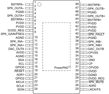
Pin Functions
| PIN | TYPE(1) | INTERNAL TERMINATION | DESCRIPTION | |
|---|---|---|---|---|
| NAME | NO. | |||
| ADR0 | 26 | DI | Sets the LSB of the I2C address to 0 if pulled to GND, to 1 if pulled to DVDD | |
| ADR1 | 20 | DI | Sets the second LSB of the I2C address to 0 if pulled to GND, to 1 if pulled to DVDD | |
| AGND | 10 | G | — | Ground reference for analog circuitry(2) |
| 15 | ||||
| AVDD | 14 | P | Figure 2 | Power supply for internal analog circuitry |
| BSTRPA– | 1 | P | Figure 3 | Connection point for the SPK_OUTA– bootstrap capacitor which is used to create a power supply for the high-side gate drive for SPK_OUTA– |
| BSTRPA+ | 5 | P | Connection point for the SPK_OUTA+ bootstrap capacitor which is used to create a power supply for the high-side gate drive for SPK_OUTA+ | |
| BSTRPB– | 48 | P | Connection point for the SPK_OUTB– bootstrap capacitor which is used to create a power supply for the high-side gate drive for SPK_OUTB– | |
| BSTRPB+ | 44 | P | Connection point for the SPK_OUTB+ bootstrap capacitor which is used to create a power supply for the high-side gate drive for SPK_OUTB+ | |
| CN | 34 | P | Figure 14 | Negative pin for capacitor connection used in the line-driver charge pump |
| CP | 32 | P | Figure 13 | Positive pin for capacitor connection used in the line-driver charge pump |
| CPVDD | 31 | P | Figure 2 | Power supply for charge pump circuitry |
| CPVSS | 35 | P | Figure 14 | –3.3-V supply generated by charge pump for the DAC |
| DAC_OUTA | 13 | AO | Figure 8 | Single-ended output for Channel A of the DAC |
| DAC_OUTB | 36 | AO | Single-ended output for Channel B of the DAC | |
| DGND | 29 | G | — | Ground reference for digital circuitry. Connect this pin to the system ground. |
| DVDD | 30 | P | Figure 2 | Power supply for the internal digital circuitry |
| DVDD_REG | 28 | P | Figure 15 | Voltage regulator derived from DVDD supply for use for internal digital circuitry. This pin is provided as a connection point for filtering capacitors for this supply and must not be used to power any external circuitry. |
| GND | 33 | G | — | Ground pin for device. This pin should be connected to the system ground. |
| GPIO0 | 18 | DI/O | General purpose input/output pins (GPIOx). Refer to GPIO registers for configuration. | |
| GPIO2 | 21 | |||
| GVDD_REG | 8 | P | Figure 5 | Voltage regulator derived from PVDD supply to generate the voltage required for the gate drive of output MOSFETs. This pin is provided as a connection point for filtering capacitors for this supply and must not be used to power any external circuitry. |
| LRCK/FS | 25 | DI/O | Figure 11 | Word select clock for the digital signal that is active on the serial port's input data line. In I2S, LJ, and RJ, this corresponds to the left channel and right channel boundary. In TDM mode, this corresponds to the frame sync boundary. |
| MCLK | 22 | DI | Master clock used for internal clock tree and sub-circuit and state machine clocking | |
| PGND | 3 | G | — | Ground reference for power device circuitry. Connect this pin to the system ground. |
| 39 | ||||
| 46 | ||||
| PVDD | 6 | P | Figure 1 | Power supply for internal power circuitry |
| 7 | ||||
| 41 | ||||
| 42 | ||||
| 43 | ||||
| RESET | 19 | DI | Figure 17 | Device reset input. Pull down to reset, pull up to activate device. |
| SCL | 17 | DI | Figure 10 | I2C serial control port clock |
| SCLK | 23 | DI/O | Figure 11 | Bit clock for the digital signal that is active on the input data line of the serial data port |
| SDA | 16 | DI/O | Figure 9 | I2C serial control port data |
| SDIN | 24 | D1 | Figure 11 | Data line to the serial data port |
| SPK_INA– | 11 | AI | Figure 7 | Negative pin for differential speaker amplifier input A |
| SPK_INA+ | 12 | AI | Positive pin for differential speaker amplifier input A | |
| SPK_INB– | 38 | AI | Negative pin for differential speaker amplifier input B | |
| SPK_INB+ | 37 | AI | Positive pin for differential speaker amplifier input B | |
| SPK_FAULT | 40 | DO | Figure 16 | Fault pin which is pulled low when an overcurrent or overtemperature fault occurs |
| SPK_GAIN/FREQ | 9 | AI | Figure 6 | Sets the gain and switching frequency of the speaker amplifier, latched in upon start-up of the device. |
| SPK_OUTA– | 2 | AO | Figure 4 | Negative pin for differential speaker amplifier output A |
| SPK_OUTA+ | 4 | AO | Positive pin for differential speaker amplifier output A | |
| SPK_OUTB– | 47 | AO | Negative pin for differential speaker amplifier output B | |
| SPK_OUTB+ | 45 | AO | Positive pin for differential speaker amplifier output B | |
| SPK_MUTE | 27 | I | Figure 12 | Speaker amplifier mute which must be pulled low (connected to DGND) to mute the device and pulled high (connected to DVDD) to unmute the device. |
| PowerPAD | — | G | — | Provides both electrical and thermal connection from the device to the board. A matching ground pad must be provided on the PCB and the device connected to it through solder. For proper electrical operation, this ground pad must be connected to the system ground. |
6.1 Internal Pin Configurations
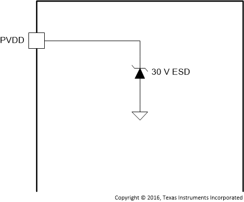 Figure 1. PVDD Pins
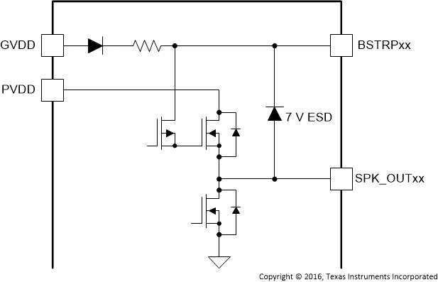 Figure 3. BSTRPxx Pins
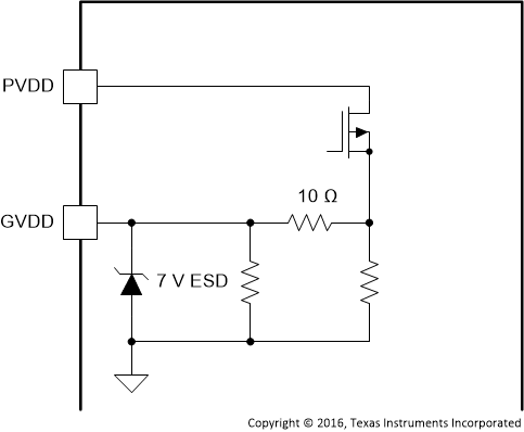 Figure 5. GVDD_REG Pin
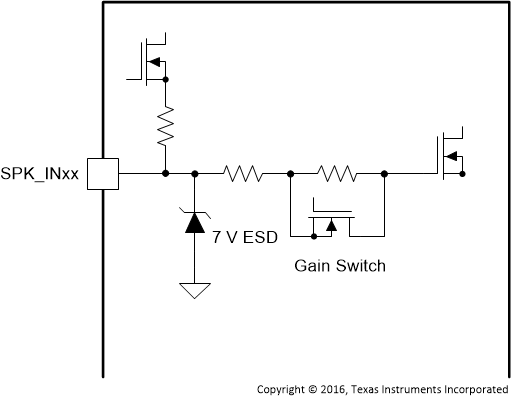 Figure 7. SPK_INxx Pins
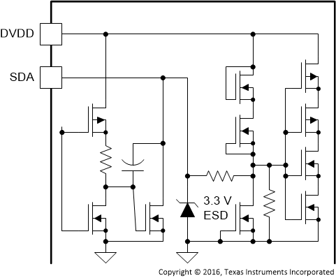 Figure 9. SDA Pin
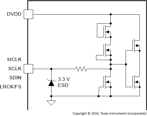 Figure 11. SCLK, BCLK, SDIN, and LRCK/FS Pins
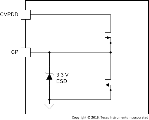 Figure 13. CP Pin
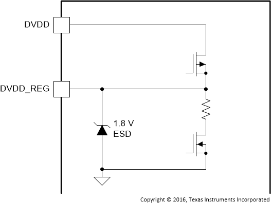 Figure 15. DVDD_REG Pin
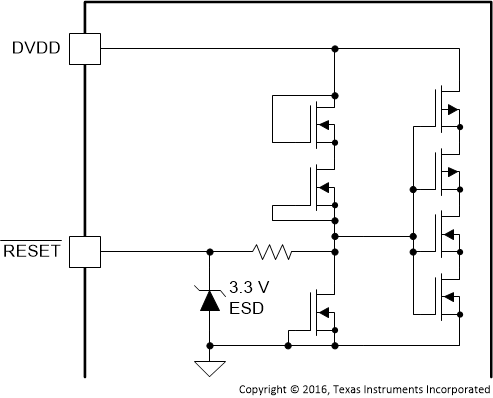 Figure 17. RESET Pin
 Figure 2. AVDD, DVDD and CPVDD Pins
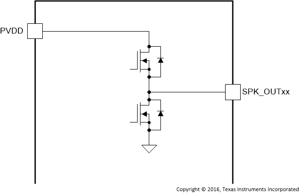 Figure 4. SPK_OUTxx Pins
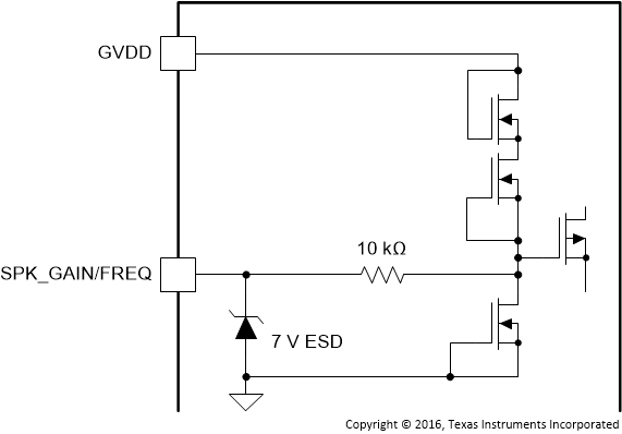 Figure 6. SPK_GAIN/FREQ Pin
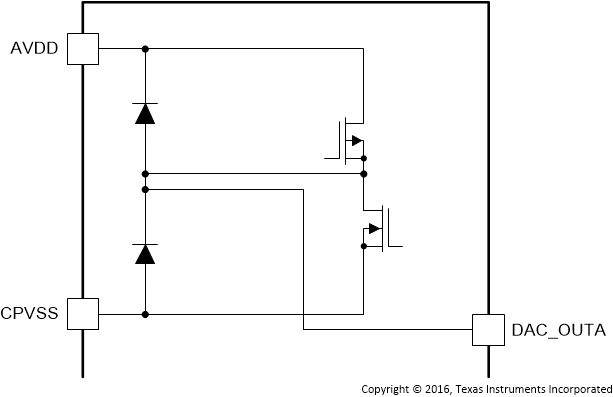 Figure 8. DAC_OUTx Pins
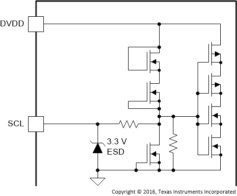 Figure 10. SCL Pin
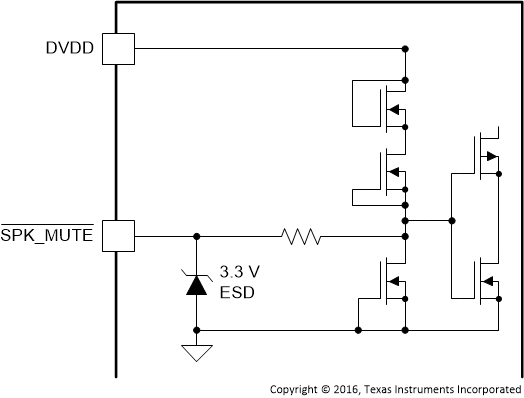 Figure 12. SPK_MUTE Pin
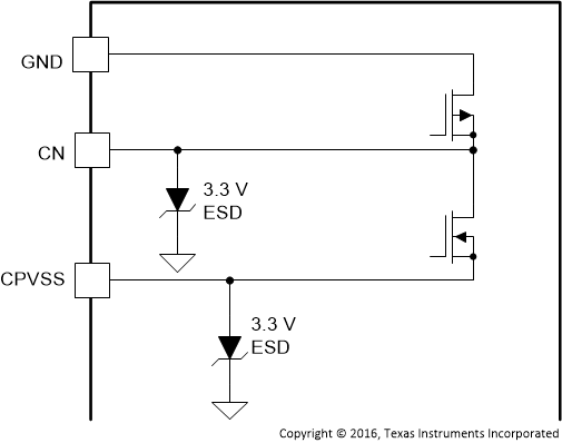 Figure 14. CN and CPVSS Pins
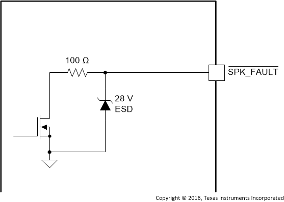 Figure 16. SPK_FAULT Pin
7 Specifications
7.1 Absolute Maximum Ratings
Free-air room temperature 25°C (unless otherwise noted)(1)| MIN | MAX | UNIT | ||
|---|---|---|---|---|
| DVDD, AVDD, CPVDD | Low-voltage digital, analog, charge pump supply | –0.3 | 3.9 | V |
| PVDD | PVDD supply | –0.3 | 30 | V |
| VI(AmpCtrl) | Input voltage for SPK_GAIN/FREQ and SPK_FAULT pins | –0.3 | VGVDD + 0.3 | V |
| VI(DigIn) | DVDD referenced digital inputs(2) | –0.5 | VDVDD + 0.5 | V |
| VI(SPK_INxx) | Analog input into speaker amplifier | –0.3 | 6.3 | V |
| VI(SPK_OUTxx) | Voltage at speaker output pins | –0.3 | 32 | V |
| Ambient operating temperature, TA | –25 | 85 | °C | |
| TJ | Operating junction temperature, digital die | –40 | 125 | °C |
| Operating junction temperature, power die | –40 | 165 | °C | |
| Tstg | Storage temperature | –40 | 125 | °C |
7.2 ESD Ratings
| VALUE | UNIT | |||
|---|---|---|---|---|
| V(ESD) | Electrostatic discharge | Human-body model (HBM), per ANSI/ESDA/JEDEC JS-001(1) | ±2000 | V |
| Charged-device model (CDM), per JEDEC specification JESD22-C101(2) | ±500 | |||
7.3 Recommended Operating Conditions
Free-air room temperature 25°C (unless otherwise noted)| MIN | NOM | MAX | UNIT | |||
|---|---|---|---|---|---|---|
| V(POWER) | Power supply inputs | DVDD, AVDD, CPVDD | 2.9 | 3.63 | V | |
| PVDD | 4.5 | 26.4 | ||||
| RSPK | Minimum speaker load | BTL Mode | 3 | Ω | ||
| PBTL Mode | 2 | Ω | ||||
| VIH(DigIn) | Input logic high for DVDD referenced digital inputs(2)(1) | 0.9 × VDVDD | VDVDD | V | ||
| VIL(DigIn) | Input logic low for DVDD referenced digital inputs(2)(2) | VDVDD | 0 | 0.1 × VDVDD | V | |
| LOUT | Minimum inductor value in LC filter under short-circuit condition | 1 | 4.7 | µH | ||
7.4 Thermal Information
| THERMAL METRIC(1) | TAS5780M
DCA (TSSOP) 48 PINS |
UNIT | |||
|---|---|---|---|---|---|
| JEDEC STANDARD 2-LAYER PCB |
JEDEC STANDARD 4-LAYER PCB |
TAS5780MEVM
4-LAYER PCB |
|||
| RθJA | Junction-to-ambient thermal resistance | 41.8 | 27.6 | 19.4 | °C/W |
| RθJC(top) | Junction-to-case (top) thermal resistance | 14.4 | 14.4 | 14.4 | °C/W |
| RθJB | Junction-to-board thermal resistance | 9.4 | 9.4 | 9.4 | °C/W |
| ψJT | Junction-to-top characterization parameter | 0.6 | 0.6 | 2 | °C/W |
| ψJB | Junction-to-board characterization parameter | 8.1 | 9.3 | 4.8 | °C/W |
| RθJC(bot) | Junction-to-case (bottom) thermal resistance | N/A | N/A | N/A | °C/W |
7.5 Electrical Characteristics
Free-air room temperature 25°C (unless otherwise noted) Measurements were made using TAS5780MEVM board and Audio Precision System 2722 with Analog Analyzer filter set to 40 kHz brickwall filter. The device output PWM frequency was set to 768 kHz unless otherwise noted.| PARAMETER | TEST CONDITIONS | MIN | TYP | MAX | UNIT | |
|---|---|---|---|---|---|---|
| DIGITAL I/O | ||||||
| |IIH|1 | Input logic high current level for DVDD referenced digital input pins(2) | VIN(DigIn) = VDVDD | 10 | µA | ||
| |IIL|1 | Input logic low current level for DVDD referenced digital input pins(2) | VIN(DigIn) = 0 V | –10 | µA | ||
| VIH1 | Input logic high threshold for DVDD referenced digital inputs(2) | 70% | VDVDD | |||
| VIL1 | Input logic low threshold for DVDD referenced digital inputs(2) | 30% | VDVDD | |||
| VOH(DigOut) | Output logic high voltage level(2) | IOH = 4 mA | 80% | VDVDD | ||
| VOL(DigOut) | Output logic low voltage level(2) | IOH = –4 mA | 22% | VDVDD | ||
| VOL(SPK_FAULT) | Output logic low voltage level for SPK_FAULT | With 100-kΩ pullup resistor | 0.8 | V | ||
| GVDD_REG | GVDD regulator voltage | 7 | V | |||
| I2C CONTROL PORT | ||||||
| CL(I2C) | Allowable load capacitance for each I2C Line | 400 | pF | |||
| fSCL(fast) | Support SCL frequency | No wait states, fast mode | 400 | kHz | ||
| fSCL(slow) | Support SCL frequency | No wait states, slow mode | 100 | kHz | ||
| VNH | Noise margin at High level for each connected device (including hysteresis) | 0.2 × VDD | V | |||
| MCLK AND PLL SPECIFICATIONS | ||||||
| DMCLK | Allowable MCLK duty cycle | 40% | 60% | |||
| fMCLK | Supported MCLK frequencies | Up to 50 MHz | 128 | 512 | fS(1) | |
| fPLL | PLL input frequency | Clock divider uses fractional divide D > 0, P = 1 |
6.7 | 20 | MHz | |
| Clock divider uses integer divide D = 0, P = 1 |
1 | 20 | ||||
| SERIAL AUDIO PORT | ||||||
| tDLY | Required LRCK/FS to SCLK rising edge delay | 5 | ns | |||
| DSCLK | Allowable SCLK duty cycle | 40% | 60% | |||
| fS | Supported input sample rates | 8 | 96 | kHz | ||
| fSCLK | Supported SCLK frequencies | 32 | 64 | fS(1) | ||
| fSCLK | SCLK frequency | Either master mode or slave mode | 24.576 | MHz | ||
| SPEAKER AMPLIFIER (ALL OUTPUT CONFIGURATIONS) | ||||||
| AV(SPK_AMP) | Speaker amplifier gain | SPK_GAIN/FREQ voltage < 3 V, see Adjustable Amplifier Gain and Switching Frequency Selection |
20 | dBV | ||
| SPK_GAIN/FREQ voltage > 3.3 V, see Adjustable Amplifier Gain and Switching Frequency Selection |
26 | |||||
| ΔAV(SPK_AMP) | Typical variation of speaker amplifier gain | ±1 | dBV | |||
| fSPK_AMP | Switching frequency of the speaker amplifier | Switching frequency depends on voltage presented at SPK_GAIN/FREQ pin and the clocking arrangement, including the incoming sample rate, see Adjustable Amplifier Gain and Switching Frequency Selection | 176.4 | 768 | kHz | |
| KSVR | Power supply rejection ratio | Injected Noise = 50 Hz to 60 Hz, 200 mVP-P, Gain = 26 dB, input audio signal = digital zero | 60 | dB | ||
| rDS(on) | Drain-to-source on resistance of the individual output MOSFETs | VPVDD = 24 V, I(SPK_OUT) = 500 mA, TJ = 25°C, includes PVDD/PGND pins, leadframe, bondwires and metallization layers. | 120 | mΩ | ||
| VPVDD = 24 V, I(SPK_OUT) = 500 mA, TJ = 25°C | 90 | |||||
| OCETHRES | SPK_OUTxx overcurrent error threshold | 7.5 | A | |||
| OTETHRES | Overtemperature error threshold | 165 | °C | |||
| OCECLRTIME | Time required to clear overcurrent error after error condition is removed. | 1.3 | s | |||
| OTECLRTIME | Time required to clear overtemperature error after error condition is removed. | 1.3 | s | |||
| OVETHRES(PVDD) | PVDD overvoltage error threshold | 27 | V | |||
| UVETHRES(PVDD) | PVDD undervoltage error threshold | 4.3 | V | |||
| SPEAKER AMPLIFIER (STEREO BTL) | ||||||
| |VOS| | Amplifier offset voltage | Measured differentially with zero input data, SPK_GAIN/FREQ pin configured for 20 dB gain, VPVDD = 12 V | 2 | mV | ||
| Measured differentially with zero input data, SPK_GAIN/FREQ pin configured for 26 dB gain, VPVDD = 24 V | 5 | 15 | ||||
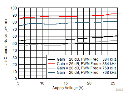
| ICN(SPK) | Idle channel noise | VPVDD = 12 V, SPK_GAIN = 20 dB, RSPK = 8 Ω, A-Weighted | 49 | µVRMS | ||
| VPVDD = 15 V, SPK_GAIN = 20 dB, RSPK = 8 Ω, A-Weighted | 59 | |||||
| VPVDD = 19 V, SPK_GAIN = 26 dB, RSPK = 8 Ω, A-Weighted | 81 | |||||
| VPVDD = 24 V, SPK_GAIN = 26 dB, RSPK = 8 Ω, A-Weighted | 82 | |||||
| PO(SPK) | Output Power (Per Channel) | VPVDD = 12 V, SPK_GAIN = 20 dB, RSPK = 4 Ω, THD+N = 0.1% | 14 | W | ||
| VPVDD = 12 V, SPK_GAIN = 20 dB, RSPK = 8 Ω, THD+N = 0.1% | 8 | |||||
| VPVDD = 15 V, SPK_GAIN = 26 dB, RSPK = 4 Ω, THD+N = 0.1% | 23 | |||||
| VPVDD = 15 V, SPK_GAIN = 26 dB, RSPK = 8 Ω, THD+N = 0.1% | 13 | |||||
| VPVDD = 19 V, SPK_GAIN = 26 dB, RSPK = 4 Ω, THD+N = 0.1% | 34 | |||||
| VPVDD = 19 V, SPK_GAIN = 26 dB, RSPK = 8 Ω, THD+N = 0.1% | 20 | |||||
| VPVDD = 24 V, SPK_GAIN = 26 dB, RSPK = 4 Ω, THD+N = 0.1% | 40 | |||||
| VPVDD = 24 V, SPK_GAIN = 26 dB, RSPK = 8 Ω, THD+N = 0.1% | 33 | |||||
| SNR | Signal-to-noise ratio (referenced to 0 dBFS input signal) | VPVDD = 12 V, SPK_GAIN = 20 dB, RSPK = 8 Ω, A-Weighted, –120 dBFS Input | 103 | dB | ||
| VPVDD = 15 V, SPK_GAIN = 26 dB, RSPK = 8 Ω, A-Weighted, –120 dBFS Input | 102 | |||||
| VPVDD = 19 V, SPK_GAIN = 26 dB, RSPK = 8 Ω, A-Weighted, –120 dBFS Input | 103 | |||||
| VPVDD = 24 V, SPK_GAIN = 26 dB, RSPK = 8 Ω, A-Weighted, –120 dBFS Input | 105 | |||||
| THD+NSPK | Total harmonic distortion and noise | VPVDD = 12 V, SPK_GAIN = 20 dB, RSPK = 4 Ω, PO = 1 W, f = 1kHz | 0.021% | |||
| VPVDD = 12 V, SPK_GAIN = 20 dB, RSPK = 8 Ω, PO = 1 W, f = 1kHz | 0.022% | |||||
| VPVDD = 15 V, SPK_GAIN = 26 dB, RSPK = 4 Ω, PO = 1 W, f = 1kHz | 0.02% | |||||
| VPVDD = 15 V, SPK_GAIN = 26 dB, RSPK = 8 Ω, PO = 1 W, f = 1kHz | 0.037% | |||||
| VPVDD = 19 V, SPK_GAIN = 26 dB, RSPK = 4 Ω, PO = 1 W, f = 1kHz | 0021% | |||||
| VPVDD = 19 V, SPK_GAIN = 26 dB, RSPK = 8 Ω, PO = 1 W, f = 1kHz | 0.028% | |||||
| VPVDD = 24 V, SPK_GAIN = 26 dB, RSPK = 4 Ω, PO = 1 W, f = 1kHz | 0.027% | |||||
| VPVDD = 24 V, SPK_GAIN = 26 dB, RSPK = 8 Ω, PO = 1 W, f = 1kHz | 0.038% | |||||
| X-talkSPK | Cross-talk (worst case between left-to-right and right-to-left coupling) | VPVDD = 12 V, SPK_GAIN = 20 dB, RSPK = 8 Ω, Input Signal 250 mVrms, 1-kHz Sine, across f(S) |
–90 | dB | ||
| VPVDD = 15 V, SPK_GAIN = 26 dBV, RSPK = 8 Ω, Input Signal 250 mVrms, 1-kHz Sine, across f(S) |
–102 | |||||
| VPVDD = 19 V, SPK_GAIN = 26 dBV, RSPK = 8 Ω, Input Signal 250 mVrms, 1-kHz Sine, across f(S) |
–93 | |||||
| VPVDD = 24 V, SPK_GAIN = 26 dBV, RSPK = 8 Ω, Input Signal 250 mVrms, 1-kHz Sine, across f(S) |
–93 | |||||
| SPEAKER AMPLIFIER (MONO PBTL) | ||||||
| |VOS| | Amplifier offset voltage | Measured differentially with zero input data, SPK_GAIN/FREQ pin configured for 20 dB gain, VPVDD = 12 V | 0.7 | mV | ||
| Measured differentially with zero input data, SPK_GAIN/FREQ pin configured for 26 dB gain, VPVDD = 24 V | 4 | |||||
| ICN | Idle channel noise | VPVDD = 12 V, SPK_GAIN = 20 dB, RSPK = 8 Ω, A-Weighted | 48 | µVRMS | ||
| VPVDD = 15 V, SPK_GAIN = 20 dB, RSPK = 8 Ω, A-Weighted | 49 | |||||
| VPVDD = 19 V, SPK_GAIN = 26 dB, RSPK = 8 Ω, A-Weighted | 83 | |||||
| VPVDD = 24 V, SPK_GAIN = 26 dB, RSPK = 8 Ω, A-Weighted | 82 | |||||
| PO | Output power (per channel) | VPVDD = 12 V, SPK_GAIN = 20 dB, RSPK = 2 Ω, THD+N = 0.1%, Unless otherwise noted | 30 | W | ||
| VPVDD = 12 V, SPK_GAIN = 20 dB, RSPK = 4 Ω, THD+N = 0.1%, Unless otherwise noted | 16 | |||||
| VPVDD = 12 V, SPK_GAIN = 20 dB, RSPK = 8 Ω, THD+N = 0.1% | 9 | |||||
| VPVDD = 15 V, SPK_GAIN = 26 dB, RSPK = 2 Ω, THD+N = 0.1%, Unless otherwise noted | 44 | |||||
| VPVDD = 15 V, SPK_GAIN = 26 dB, RSPK = 4 Ω, THD+N = 0.1%, Unless otherwise noted | 22 | |||||
| VPVDD = 15 V, SPK_GAIN = 26 dB, RSPK = 8 Ω, THD+N = 0.1% | 13 | |||||
| VPVDD = 19 V, SPK_GAIN = 26 dB, RSPK = 2 Ω, THD+N = 0.1%, Unless otherwise noted | 50 | |||||
| VPVDD = 19 V, SPK_GAIN = 26 dB, RSPK = 4 Ω, THD+N = 0.1%, Unless otherwise noted | 36 | |||||
| VPVDD = 19 V, SPK_GAIN = 26 dB, RSPK = 8 Ω, THD+N = 0.1% | 20 | |||||
| VPVDD = 24 V, SPK_GAIN = 26 dB, RSPK = 2 Ω, THD+N = 0.1%, Unless otherwise noted | 40 | |||||
| VPVDD = 24 V, SPK_GAIN = 26 dB, RSPK = 4 Ω, THD+N = 0.1%, Unless otherwise noted | 61 | |||||
| VPVDD = 24 V, SPK_GAIN = 26 dB, RSPK = 8 Ω, THD+N = 0.1% | 34 | |||||
| SNR | Signal-to-noise ratio (referenced to 0 dBFS input signal) |
VPVDD = 12 V, SPK_GAIN = 20 dB, RSPK = 8 Ω, A-Weighted, –120 dBFS Input | 105 | dB | ||
| VPVDD = 15 V, SPK_GAIN = 26 dB, RSPK = 8 Ω, A-Weighted, –120 dBFS Input | 104 | |||||
| VPVDD = 19 V, SPK_GAIN = 26 dB, RSPK = 8 Ω, A-Weighted, –120 dBFS Input | 105 | |||||
| VPVDD = 24 V, SPK_GAIN = 26 dB, RSPK = 8 Ω, A-Weighted, –120 dBFS Input | 107 | |||||
| THD+N | Total harmonic distortion and noise | VPVDD = 12 V, SPK_GAIN = 20 dB, RSPK = 2 Ω, PO = 1 W, f = 1kHz | 0.014% | |||
| VPVDD = 12 V, SPK_GAIN = 20 dB, RSPK = 4 Ω, PO = 1 W, f = 1kHz | 0.011% | |||||
| VPVDD = 12 V, SPK_GAIN = 20 dB, RSPK = 8 Ω, PO = 1 W, f = 1kHz | 0.014% | |||||
| VPVDD = 15 V, SPK_GAIN = 26 dB, RSPK = 2 Ω, PO = 1 W, f = 1kHz | 0.015% | |||||
| VPVDD = 15 V, SPK_GAIN = 26 dB, RSPK = 4 Ω, PO = 1 W, f = 1kHz | 0.013% | |||||
| VPVDD = 15 V, SPK_GAIN = 26 dB, RSPK = 8 Ω, PO = 1 W, f = 1kHz | 0.015% | |||||
| VPVDD = 19 V, SPK_GAIN = 26 dB, RSPK = 2 Ω, PO = 1 W, f = 1kHz | 0.018% | |||||
| V, RSPK = 4 Ω, PO = 1 W, f = 1kHz | 0.012% | |||||
| VPVDD = 19 V, SPK_GAIN = 26 dB, RSPK = 8 Ω, PO = 1 W, f = 1kHz | 0.020% | |||||
| VPVDD = 24 V, SPK_GAIN = 26 dB, RSPK = 2 Ω, PO = 1 W, f = 1kHz | 0.028% | |||||
| VPVDD = 24 V, SPK_GAIN = 26 dB, RSPK = 4 Ω, PO = 1 W, f = 1kHz | 0.02% | |||||
| VPVDD = 24 V, SPK_GAIN = 26 dB, RSPK = 8 Ω, PO = 1 W, f = 1kHz | 0.027% | |||||
7.6 Power Dissipation Characteristics
Free-air room temperature 25°C (unless otherwise noted)| VPVDD
(V) |
SPK_GAIN(1)(2)(3)
(dBV) |
fSPK_AMP
(kHz) |
STATE OF OPERATION |
RSPK
(Ω) |
IPVDD(4)
(mA) |
IDVDD(5)
(mA) |
PDISS
(W) |
|---|---|---|---|---|---|---|---|
| 7.4 | 20 | 384 | Idle | 4 | 21.30 | 59.70 | 0.355 |
| 6 | 21.33 | 59.68 | 0.355 | ||||
| 8 | 21.30 | 59.70 | 0.355 | ||||
| Mute | 4 | 21.33 | 58.82 | 0.352 | |||
| 6 | 21.34 | 58.81 | 0.352 | ||||
| 8 | 21.36 | 58.81 | 0.352 | ||||
| Standby | 4 | 2.08 | 12.41 | 0.056 | |||
| 6 | 2.11 | 12.41 | 0.057 | ||||
| 8 | 2.17 | 12.41 | 0.057 | ||||
| Powerdown | 4 | 2.03 | 0.730 | 0.017 | |||
| 6 | 2.04 | 0.740 | 0.018 | ||||
| 8 | 2.06 | 0.740 | 0.018 | ||||
| 768 | Idle | 4 | 27.48 | 59.7 | 0.400 | ||
| 6 | 27.49 | 59.73 | 0.401 | ||||
| 8 | 24.46 | 59.72 | 0.378 | ||||
| Mute | 4 | 27.50 | 58.8 | 0.398 | |||
| 6 | 27.51 | 58.8 | 0.398 | ||||
| 8 | 27.52 | 58.81 | 0.398 | ||||
| Standby | 4 | 2.04 | 12.41 | 0.056 | |||
| 6 | 2.08 | 12.41 | 0.056 | ||||
| 8 | 2.11 | 12.41 | 0.057 | ||||
| Powerdown | 4 | 2.06 | 0.73 | 0.018 | |||
| 6 | 2.07 | 0.74 | 0.018 | ||||
| 8 | 2.08 | 0.74 | 0.018 | ||||
| 11.1 | 20 | 384 | Idle | 4 | 24.33 | 59.74 | 0.467 |
| 6 | 24.32 | 59.74 | 0.467 | ||||
| 8 | 24.36 | 59.70 | 0.467 | ||||
| Mute | 4 | 24.36 | 58.81 | 0.464 | |||
| 6 | 24.32 | 58.82 | 0.464 | ||||
| 8 | 24.37 | 58.84 | 0.465 | ||||
| Standby | 4 | 3.58 | 12.40 | 0.081 | |||
| 6 | 3.57 | 12.41 | 0.081 | ||||
| 8 | 3.58 | 12.42 | 0.081 | ||||
| Powerdown | 4 | 3.52 | 0.74 | 0.042 | |||
| 6 | 3.52 | 0.74 | 0.042 | ||||
| 8 | 3.54 | 0.74 | 0.042 | ||||
| 768 | Idle | 4 | 30.70 | 59.70 | 0.538 | ||
| 6 | 30.65 | 59.72 | 0.537 | ||||
| 8 | 30.67 | 59.71 | 0.537 | ||||
| Mute | 4 | 3.072 | 58.80 | 0.528 | |||
| 6 | 30.69 | 58.81 | 0.535 | ||||
| 8 | 30.69 | 58.81 | 0.535 | ||||
| Standby | 4 | 3.54 | 12.40 | 0.080 | |||
| 6 | 3.54 | 12.41 | 0.080 | ||||
| 8 | 3.58 | 12.42 | 0.081 | ||||
| Powerdown | 4 | 3.53 | 0.74 | 0.042 | |||
| 6 | 3.53 | 0.74 | 0.042 | ||||
| 8 | 3.55 | 0.74 | 0.042 | ||||
| 12 | 20 | 384 | Idle | 4 | 25.07 | 59.72 | 0.498 |
| 6 | 25.08 | 59.73 | 0.498 | ||||
| 8 | 25.10 | 59.71 | 0.498 | ||||
| Mute | 4 | 25.12 | 58.84 | 0.496 | |||
| 6 | 25.08 | 58.82 | 0.495 | ||||
| 8 | 25.11 | 58.82 | 0.495 | ||||
| Standby | 4 | 3.92 | 12.40 | 0.088 | |||
| 6 | 3.93 | 12.41 | 0.088 | ||||
| 8 | 3.94 | 12.41 | 0.088 | ||||
| Powerdown | 4 | 3.87 | 0.75 | 0.049 | |||
| 6 | 3.85 | 0.74 | 0.049 | ||||
| 8 | 3.87 | 0.75 | 0.049 | ||||
| 768 | Idle | 4 | 31.31 | 59.72 | 0.573 | ||
| 6 | 31.29 | 59.71 | 0.573 | ||||
| 8 | 31.31 | 59.74 | 0.573 | ||||
| Mute | 4 | 31.31 | 58.80 | 0.570 | |||
| 6 | 31.33 | 58.81 | 0.570 | ||||
| 8 | 31.32 | 58.81 | 0.570 | ||||
| Standby | 4 | 3.88 | 12.40 | 0.087 | |||
| 6 | 3.90 | 12.41 | 0.088 | ||||
| 8 | 3.91 | 12.41 | 0.088 | ||||
| Powerdown | 4 | 3.89 | 0.75 | 0.049 | |||
| 6 | 3.91 | 0.74 | 0.049 | ||||
| 8 | 3.88 | 0.75 | 0.049 | ||||
| 15 | 26 | 384 | Idle | 4 | 27.94 | 59.73 | 0.616 |
| 6 | 27.91 | 59.75 | 0.616 | ||||
| 8 | 27.75 | 59.69 | 0.613 | ||||
| Mute | 4 | 27.98 | 58.84 | 0.614 | |||
| 6 | 27.94 | 58.87 | 0.613 | ||||
| 8 | 27.88 | 58.85 | 0.612 | ||||
| Standby | 4 | 5.09 | 12.41 | 0.117 | |||
| 6 | 5.12 | 12.41 | 0.118 | ||||
| 8 | 5.19 | 12.41 | 0.119 | ||||
| Powerdown | 4 | 5.02 | 0.74 | 0.078 | |||
| 6 | 5.06 | 0.74 | 0.078 | ||||
| 8 | 5.14 | 0.74 | 0.080 | ||||
| 768 | Idle | 4 | 33.05 | 59.7 | 0.693 | ||
| 6 | 33.03 | 59.72 | 0.693 | ||||
| 8 | 33.08 | 59.68 | 0.693 | ||||
| Mute | 4 | 33.03 | 58.81 | 0.690 | |||
| 6 | 33.04 | 58.81 | 0.690 | ||||
| 8 | 33.05 | 58.80 | 0.690 | ||||
| Standby | 4 | 5.07 | 12.41 | 0.117 | |||
| 6 | 5.09 | 12.41 | 0.117 | ||||
| 8 | 5.14 | 12.41 | 0.118 | ||||
| Powerdown | 4 | 5.02 | 0.74 | 0.078 | |||
| 6 | 5.04 | 0.74 | 0.078 | ||||
| 8 | 5.09 | 0.74 | 0.079 | ||||
| 19.6 | 26 | 384 | Idle | 4 | 32.27 | 59.77 | 0.830 |
| 6 | 32.19 | 59.76 | 0.828 | ||||
| 8 | 32.08 | 59.75 | 0.826 | ||||
| Mute | 4 | 32.27 | 58.85 | 0.827 | |||
| 6 | 32.24 | 58.87 | 0.826 | ||||
| 8 | 32.22 | 58.86 | 0.826 | ||||
| Standby | 4 | 6.95 | 12.40 | 0.177 | |||
| 6 | 6.93 | 12.42 | 0.177 | ||||
| 8 | 7.00 | 12.41 | 0.178 | ||||
| Powerdown | 4 | 6.89 | 0.74 | 0.137 | |||
| 6 | 6.90 | 0.74 | 0.138 | ||||
| 8 | 6.96 | 0.73 | 0.139 | ||||
| 768 | Idle | 4 | 34.99 | 59.74 | 0.883 | ||
| 6 | 34.95 | 59.74 | 0.882 | ||||
| 8 | 34.97 | 59.71 | 0.882 | ||||
| Mute | 4 | 34.96 | 58.85 | 0.879 | |||
| 6 | 34.98 | 58.83 | 0.880 | ||||
| 8 | 34.96 | 58.81 | 0.879 | ||||
| Standby | 4 | 6.93 | 12.40 | 0.177 | |||
| 6 | 6.93 | 12.42 | 0.177 | ||||
| 8 | 6.98 | 12.41 | 0.178 | ||||
| Powerdown | 4 | 6.84 | 0.74 | 0.137 | |||
| 6 | 6.89 | 0.74 | 0.137 | ||||
| 8 | 6.90 | 0.73 | 0.138 | ||||
| 24 | 26 | 384 | Idle | 4 | 36.93 | 59.80 | 1.084 |
| 6 | 36.87 | 59.81 | 1.082 | ||||
| 8 | 36.77 | 59.76 | 1.080 | ||||
| Mute | 4 | 36.94 | 58.91 | 1.081 | |||
| 6 | 36.89 | 58.89 | 1.080 | ||||
| 8 | 36.85 | 58.90 | 1.079 | ||||
| Standby | 4 | 8.73 | 12.40 | 0.250 | |||
| 6 | 8.72 | 12.40 | 0.250 | ||||
| 8 | 8.71 | 12.40 | 0.250 | ||||
| Powerdown | 4 | 8.64 | 0.74 | 0.210 | |||
| 6 | 8.66 | 0.74 | 0.210 | ||||
| 8 | 8.69 | 0.73 | 0.211 | ||||
| 768 | Idle | 4 | 36.84 | 59.73 | 1.081 | ||
| 6 | 36.86 | 59.76 | 1.082 | ||||
| 8 | 36.83 | 59.78 | 1.081 | ||||
| Mute | 4 | 36.85 | 58.85 | 1.079 | |||
| 6 | 36.84 | 58.84 | 1.078 | ||||
| 8 | 36.82 | 58.83 | 1.078 | ||||
| Standby | 4 | 8.66 | 12.40 | 0.249 | |||
| 6 | 8.68 | 12.40 | 0.249 | ||||
| 8 | 8.71 | 12.40 | 0.250 | ||||
| Powerdown | 4 | 8.63 | 0.74 | 0.210 | |||
| 6 | 8.64 | 0.74 | 0.210 | ||||
| 8 | 8.65 | 0.73 | 0.210 |
7.7 MCLK Timing
See Figure 18.| MIN | NOM | MAX | UNIT | ||
|---|---|---|---|---|---|
| tMCLK | MCLK period | 20 | 1000 | ns | |
| tMCLKH | MCLK pulse width, high | 9 | ns | ||
| tMCLKL | MCLK pulse width, low | 9 | ns | ||
7.8 Serial Audio Port Timing – Slave Mode
See Figure 19.| MIN | NOM | MAX | UNIT | ||
|---|---|---|---|---|---|
| fSCLK | SCLK frequency | 1.024 | MHz | ||
| tSCLK | SCLK period | 40 | ns | ||
| tSCLKL | SCLK pulse width, low | 16 | ns | ||
| tSCLKH | SCLK pulse width, high | 16 | ns | ||
| tSL | SCLK rising to LRCK/FS edge | 8 | ns | ||
| tLS | LRCK/FS Edge to SCLK rising edge | 8 | ns | ||
| tSU | Data setup time, before SCLK rising edge | 8 | ns | ||
| tDH | Data hold time, after SCLK rising edge | 8 | ns | ||
| tDFS | Data delay time from SCLK falling edge | 15 | ns | ||
7.9 Serial Audio Port Timing – Master Mode
See Figure 20.| MIN | NOM | MAX | UNIT | ||
|---|---|---|---|---|---|
| tSCLK | SCLK period | 40 | ns | ||
| tSCLKL | SCLK pulse width, low | 16 | ns | ||
| tSCLKH | SCLK pulse width, high | 16 | ns | ||
| tLRD | LRCK/FS delay time from to SCLK falling edge | –10 | 20 | ns | |
| tSU | Data setup time, before SCLK rising edge | 8 | ns | ||
| tDH | Data hold time, after SCLK rising edge | 8 | ns | ||
| tDFS | Data delay time from SCLK falling edge | 15 | ns | ||
7.10 I2C Bus Timing – Standard
| MIN | MAX | UNIT | ||
|---|---|---|---|---|
| fSCL | SCL clock frequency | 100 | kHz | |
| tBUF | Bus free time between a STOP and START condition | 4.7 | µs | |
| tLOW | Low period of the SCL clock | 4.7 | µs | |
| tHI | High period of the SCL clock | 4 | µs | |
| tRS-SU | Setup time for (repeated) START condition | 4.7 | µs | |
| tS-HD | Hold time for (repeated) START condition | 4 | µs | |
| tD-SU | Data setup time | 250 | ns | |
| tD-HD | Data hold time | 0 | 900 | ns |
| tSCL-R | Rise time of SCL signal | 20 + 0.1CB | 1000 | ns |
| tSCL-R1 | Rise time of SCL signal after a repeated START condition and after an acknowledge bit | 20 + 0.1CB | 1000 | ns |
| tSCL-F | Fall time of SCL signal | 20 + 0.1CB | 1000 | ns |
| tSDA-R | Rise time of SDA signal | 20 + 0.1CB | 1000 | ns |
| tSDA-F | Fall time of SDA signal | 20 + 0.1CB | 1000 | ns |
| tP-SU | Setup time for STOP condition | 4 | µs | |
7.11 I2C Bus Timing – Fast
See Figure 21.| MIN | MAX | UNIT | ||
|---|---|---|---|---|
| fSCL | SCL clock frequency | 400 | kHz | |
| tBUF | Bus free time between a STOP and START condition | 1.3 | µs | |
| tLOW | Low period of the SCL clock | 1.3 | µs | |
| tHI | High period of the SCL clock | 600 | ns | |
| tRS-SU | Setup time for (repeated)START condition | 600 | ns | |
| tRS-HD | Hold time for (repeated)START condition | 600 | ns | |
| tD-SU | Data setup time | 100 | ns | |
| tD-HD | Data hold time | 0 | 900 | ns |
| tSCL-R | Rise time of SCL signal | 20 + 0.1CB | 300 | ns |
| tSCL-R1 | Rise time of SCL signal after a repeated START condition and after an acknowledge bit | 20 + 0.1CB | 300 | ns |
| tSCL-F | Fall time of SCL signal | 20 + 0.1CB | 300 | ns |
| tSDA-R | Rise time of SDA signal | 20 + 0.1CB | 300 | ns |
| tSDA-F | Fall time of SDA signal | 20 + 0.1CB | 300 | ns |
| tP-SU | Setup time for STOP condition | 600 | ns | |
| tSP | Pulse width of spike suppressed | 50 | ns | |
 Figure 18. Timing Requirements for MCLK Input
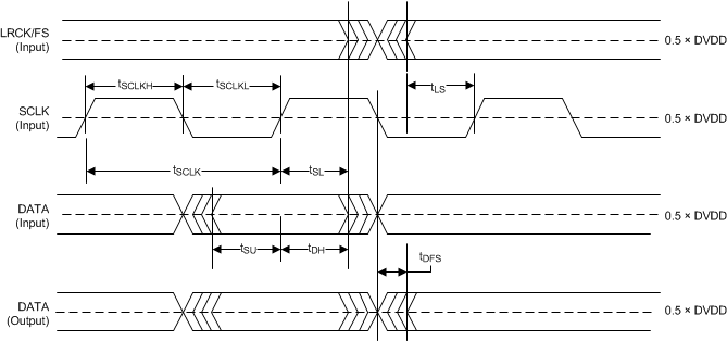 Figure 19. MCLK Timing Diagram in Slave Mode
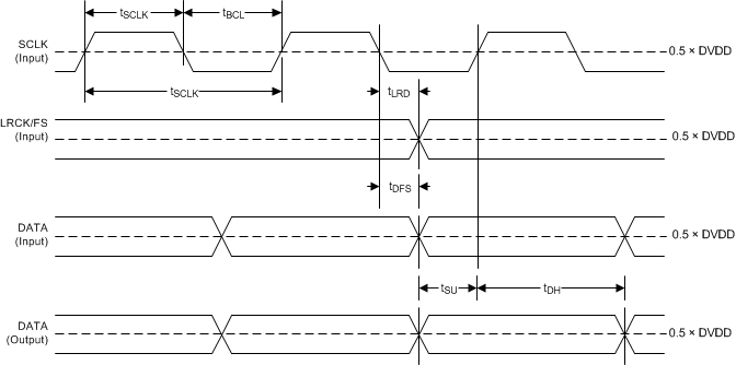 Figure 20. MCLK Timing Diagram in Master Mode
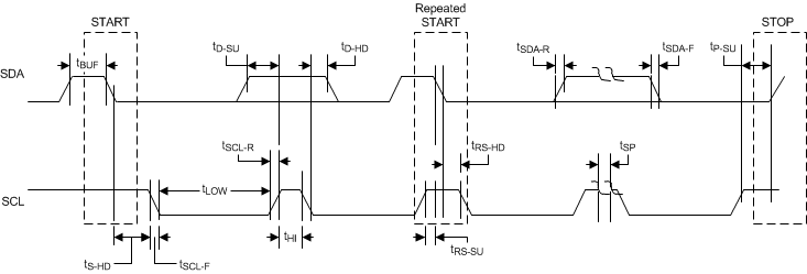 Figure 21. I2C Communication Port Timing Diagram
 Figure 22. SPK_MUTE Timing Diagram for Soft Mute Operation via Hardware Pin
7.13 Typical Characteristics
All performance plots were taken using the TAS5780MEVM Board at room temperature, unless otherwise noted. The term "traditional LC filter" refers to the output filter that is present by default on the TAS5780MEVM Board.
Table 1. Quick Reference Table
| OUTPUT CONFIGURATIONS |
PLOT TITLE | FIGURE NUMBER |
|---|---|---|
| Bridge Tied Load (BTL) Configuration Curves | Frequency Response | Figure 34 |
| Output Power vs PVDD | Figure 23 | |
| THD+N vs Frequency, VPVDD = 12 V | Figure 24 | |
| THD+N vs Frequency, VPVDD = 15 V | Figure 25 | |
| THD+N vs Frequency, VPVDD = 18 V | Figure 26 | |
| THD+N vs Frequency, VPVDD = 24 V | Figure 27 | |
| THD+N vs Power, VPVDD = 12 V | Figure 28 | |
| THD+N vs Power, VPVDD = 15 V | Figure 29 | |
| THD+N vs Power, VPVDD = 18 V | Figure 30 | |
| THD+N vs Power, VPVDD = 24 V | Figure 31 | |
| Idle Channel Noise vs PVDD | Figure 32 | |
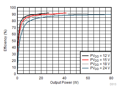
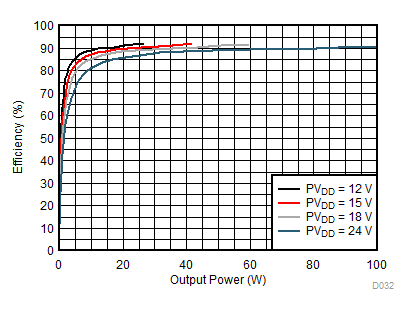
| Efficiency vs Output Power | Figure 33 | |
| Efficiency vs Output Power | Figure 34 | |
| Efficiency vs Output Power | Figure 35 | |
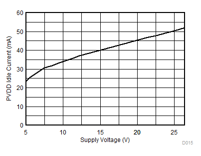
| Idle Current Draw (Filterless) vs PVDD | Figure 36 | |
| Crosstalk vs. Frequency | Figure 37 | |
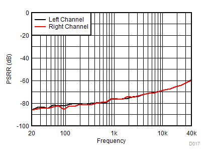
| PVDD PSRR vs Frequency | Figure 38 | |
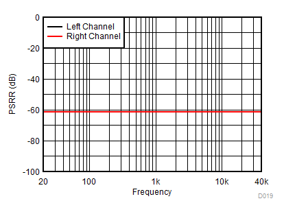
| DVDD PSRR vs Frequency | Figure 39 | |
| AVDD PSRR vs Frequency | Figure 40 | |
| CPVDD PSRR vs Frequency | Figure 41 | |
| Parallel Bridge Tied Load (PBTL) Configuration | Output Power vs PVDD | Figure 43 |
| THD+N vs Frequency, VPVDD = 12 V | Figure 44 | |
| THD+N vs Frequency, VPVDD = 15 V | Figure 45 | |
| THD+N vs Frequency, VPVDD = 18 V | Figure 46 | |
| THD+N vs Frequency, VPVDD = 24 V | Figure 47 | |
| THD+N vs Power, VPVDD = 12 V | Figure 48 | |
| THD+N vs Power, VPVDD = 15 V | Figure 49 | |
| THD+N vs Power, VPVDD = 18 V | Figure 50 | |
| THD+N vs Power, VPVDD = 24 V | Figure 51 | |
| Idle Channel Noise vs PVDD | Figure 52 | |
| Efficiency vs Output Power | Figure 53 |
7.13.1 Bridge Tied Load (BTL) Configuration Curves
Free-air room temperature 25°C (unless otherwise noted) Measurements were made using TAS5780MEVM board and Audio Precision System 2722 with Analog Analyzer filter set to 40-kHz brickwall filter. All measurements taken with audio frequency set to 1 kHz and device PWM frequency set to 768 kHz, unless otherwise noted. For both the BTL plots and the PBTL plots, the LC filter used was 4.7 µH / 0.68 µF. Return to Quick Reference Table.

| AV(SPK_AMP) = 26 dBV |

| AV(SPK_AMP) = 20 dBV | PO = 1 W | VPVDD = 15 V |
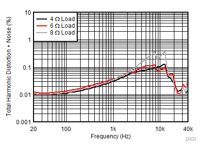
| AV(SPK_AMP) = 20 dBV | PO = 1 W | VPVDD = 12 V |
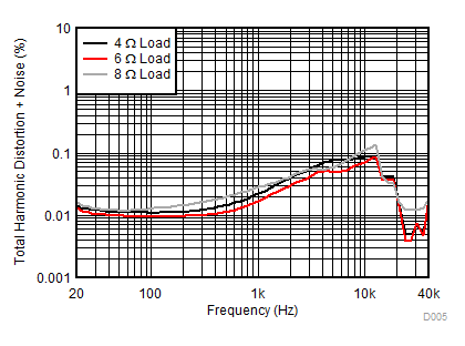
| AV(SPK_AMP) = 26 dBV | PO = 1 W | VPVDD = 18 V |

| AV(SPK_AMP) = 26 dBV | PO = 1 W | VPVDD = 24 V |
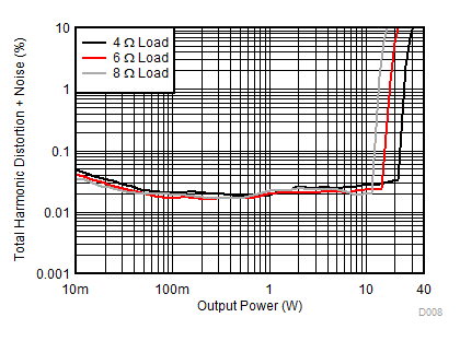
| AV(SPK_AMP) = 20 dBV | VPVDD = 15 V |
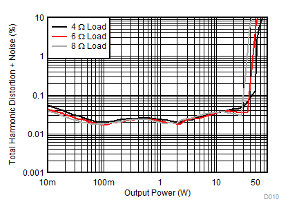
| AV(SPK_AMP) = 26 dBV | VPVDD = 24 V |
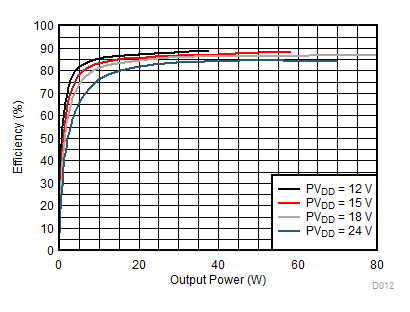
| RSPK = 4 Ω |
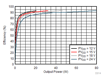
| RSPK = 8 Ω |
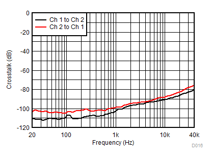
| AV(SPK_AMP) = 26 dBV | VPVDD = 24 V |
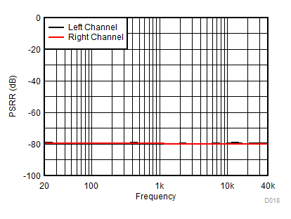
| AV(SPK_AMP) = 26 dBV | VPVDD = 24 V |
| VDVDD = 3.3 V + 250 mVac |
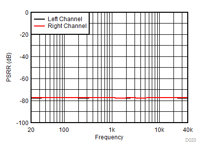
| AV(SPK_AMP) = 26 dBV | VPVDD = 24 V |
| VCPVDD = 3.3 V + 250 mVac |
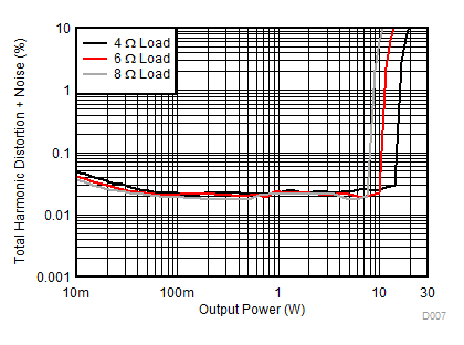
| AV(SPK_AMP) = 20 dBV | VPVDD = 12 V |
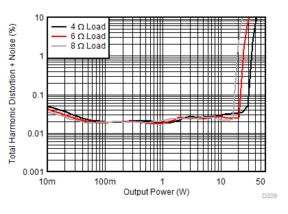
| AV(SPK_AMP) = 26 dBV | VPVDD = 18 V |
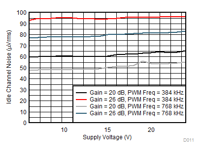
| RSPK = 4 Ω |
| RSPK = 6 Ω |
| fSPK_AMP = 768 kHz | RSPK = 8 Ω |
| AV(SPK_AMP) = 26 dBV | VPVDD = 24 V + 250 mVac |
| AV(SPK_AMP) = 26 dBV | VPVDD = 24 V |
| VAVDD = 3.3 V + 250 mVac |
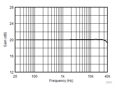
| AV(SPK_AMP) = 20 dB | PVDD = 12 V | |
7.13.2 Parallel Bridge Tied Load (PBTL) Configuration
Return to Quick Reference Table.
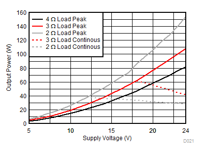
| AV(SPK_AMP) = 26 dBV | ||
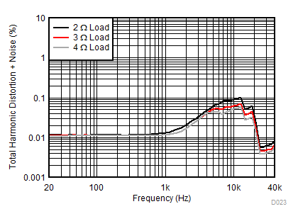
| AV(SPK_AMP) = 20 dBV | PO = 1 W | VPVDD = 15 V |
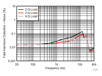
| AV(SPK_AMP) = 26 dBV | PO = 1 W | VPVDD = 24 V |
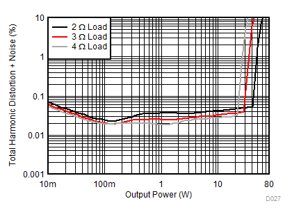
| AV(SPK_AMP) = 20 dBV
|
VPVDD = 15 V |
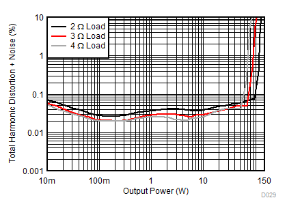
| AV(SPK_AMP) = 20 dBV
|
VPVDD = 24 V |
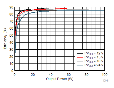
| AV(SPK_AMP) = 26 dBV | RSPK = 2 Ω |
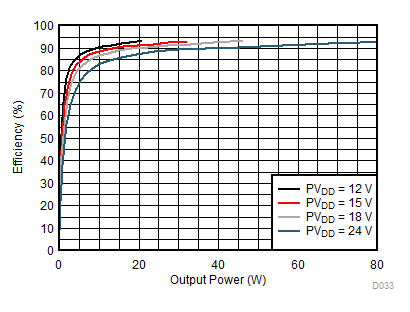
| AV(SPK_AMP) = 20 dBV | RSPK = 4 Ω |
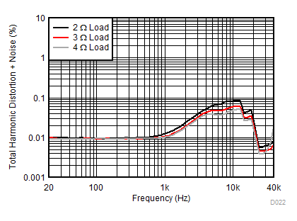
| AV(SPK_AMP) = 20 dBV | PO = 1 W | VPVDD = 12 V |
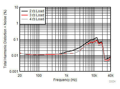
| AV(SPK_AMP) = 26 dBV | PO = 1 W | VPVDD = 18 V |
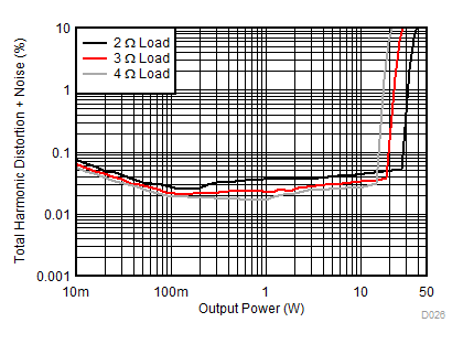
| AV(SPK_AMP) = 20 dBV | VPVDD = 12 V |
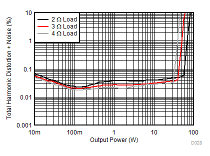
| AV(SPK_AMP) = 26 dBV
|
VPVDD = 18 V |
| RSPK = 4 Ω |
| AV(SPK_AMP) = 20 dBV | RSPK = 3 Ω |